Crosstalk Reduction in Multilayer PCB
By:PCBBUY 01/30/2026 16:30

Introduction
As signal speeds continue to increase in modern electronic systems, crosstalk has become one of the primary challenges affecting signal integrity in multilayer PCB designs. In high-density and high-speed applications, uncontrolled electromagnetic coupling between adjacent signal traces can lead to timing errors, noise, and reduced system reliability.
Effective crosstalk reduction in multilayer PCB requires not only proper design techniques but also precise manufacturing control. This article explains the mechanisms behind crosstalk, common causes in multilayer boards, and how professional PCB manufacturing processes help minimize its impact.
What Is Crosstalk in Multilayer PCB?
Crosstalk is unwanted signal coupling between neighboring conductors caused by capacitive and inductive coupling. In multilayer PCBs, it commonly appears as:
-
Near-end crosstalk (NEXT): interference at the signal source
-
Far-end crosstalk (FEXT): interference at the receiving end
The risk of crosstalk increases as trace spacing decreases, signal edge rates increase, and dielectric thickness becomes thinner.

Why Crosstalk Control Is Critical in Multilayer PCB?
Excessive crosstalk can result in:
-
Signal distortion and jitter
-
Reduced noise margins
-
Bit errors in high-speed digital systems
-
Performance degradation in mixed-signal designs
In multilayer PCB, crosstalk issues are often compounded by tight routing density and limited layer spacing.
Common Causes of Crosstalk in Multilayer PCB
|
Cause |
Description |
Impact |
|
Tight trace spacing |
Parallel traces routed too closely |
Increased capacitive coupling |
|
Long parallel routing |
Extended coupling length |
Higher NEXT and FEXT |
|
Inadequate reference planes |
Discontinuous return paths |
Unstable impedance |
|
Poor layer arrangement |
Signal layers stacked together |
Layer-to-layer coupling |
These issues often stem from both design constraints and manufacturing limitations.
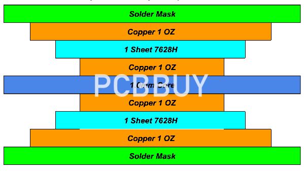
Stackup Design Strategies for Crosstalk Reduction
Proper stackup design is one of the most effective ways to reduce crosstalk:
-
Pair signal layers with solid ground planes
-
Insert ground planes between adjacent signal layers
-
Control dielectric thickness to manage field coupling
-
Maintain stackup symmetry to improve stability
Manufacturers assist by proposing optimized stackups based on material availability and lamination capability.

Trace Routing Guidelines That Influence Crosstalk
Routing techniques that help reduce crosstalk include:
-
Increasing trace-to-trace spacing where possible
-
Minimizing parallel routing length
-
Routing signals orthogonally on adjacent layers
-
Using ground guard traces with stitching vias
-
Carefully routing differential pairs
These guidelines must align with the manufacturer’s etching and registration tolerances.
Material Properties Affecting Crosstalk Performance
Material selection has a direct impact on signal coupling:
-
Dielectric constant (Dk) consistency affects impedance and coupling strength
-
Loss tangent (Df) influences signal attenuation at high frequencies
-
Resin uniformity ensures stable dielectric spacing
High-speed applications often require materials with tightly controlled dielectric properties.
Manufacturing Factors That Affect Crosstalk
Even well-designed layouts can suffer if manufacturing precision is insufficient. Key manufacturing factors include:
-
Trace width and spacing accuracy during etching
-
Dielectric thickness tolerance after lamination
-
Layer-to-layer registration accuracy
-
Copper surface roughness consistency
Strict process control helps ensure the fabricated PCB matches the intended electrical design.

Testing and Validation of Crosstalk Performance
To verify crosstalk control, manufacturers may perform:
-
Impedance and TDR measurements
-
Electrical testing on representative structures
-
Cross-section inspection for dielectric uniformity
-
Correlation with signal integrity simulations
These tests help confirm manufacturing consistency for SI-critical designs.
How PCBBUY Supports Crosstalk Reduction in Multilayer PCB?
PCBBUY supports crosstalk-sensitive designs through:
-
Stackup consultation during the design stage
-
Controlled lamination and dielectric thickness management
-
High-precision etching and registration processes
-
Experience with high-speed and multilayer PCB production
This manufacturing-focused approach helps maintain predictable signal performance.
Design Guidelines Summary for Crosstalk Reduction
-
Optimize stackup before routing
-
Use continuous reference planes
-
Increase spacing and reduce coupling length
-
Coordinate design rules with manufacturing capability
Early collaboration between designers and manufacturers is essential for success.

Conclusion
Crosstalk reduction in multilayer PCB is a combined effort involving thoughtful design and precise manufacturing. While design techniques set the foundation, manufacturing accuracy determines whether those techniques are realized in the final product.
Selecting a PCB manufacturer with proven multilayer and high-speed process control is critical for achieving reliable signal integrity.
FAQ
What causes crosstalk in multilayer PCB?
Crosstalk is caused by capacitive and inductive coupling between adjacent signal traces, especially when spacing is tight and signals run in parallel.
How does stackup design affect crosstalk?
Stackup determines the distance between signal layers and reference planes. Proper signal–ground pairing significantly reduces coupling.
Can PCB manufacturing tolerances impact crosstalk?
Yes. Variations in trace width, spacing, dielectric thickness, and layer registration can increase crosstalk beyond design expectations.
How do PCB manufacturers help reduce crosstalk?
Manufacturers provide stackup optimization, tight process control, and material selection support to ensure electrical performance targets are met.
Is crosstalk only a problem in high-speed PCB?
While more severe in high-speed designs, crosstalk can affect any dense multilayer PCB with parallel routing and insufficient spacing.
Industry Category


