
Best Practices for Reliable HDI PCB Manufacturing and High-Density Interconnect Design
By:PCBBUY 07/23/2026 15:19
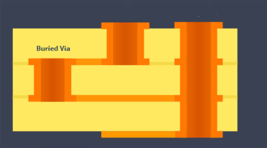
As electronic products become thinner, faster, and more compact, PCB designers are increasingly adopting blind vias and buried vias to maximize routing density while maintaining signal integrity. These advanced via structures are widely used in HDI PCBs, 5G communication equipment, AI servers, automotive electronics, aerospace systems, and medical devices.
However, simply incorporating blind and buried vias into a design is not enough. Successful manufacturing depends on proper design optimization for blind and buried vias, ensuring the PCB can be fabricated reliably, assembled efficiently, and perform consistently throughout its service life.
In this article, we'll explore the key design considerations, manufacturing challenges, and optimization strategies for blind and buried vias, while highlighting how PCBBUY supports advanced HDI PCB fabrication with precision engineering and strict quality control.
What Are Blind and Buried Vias?
Blind vias and buried vias are advanced interconnection structures used in multilayer PCBs.
-
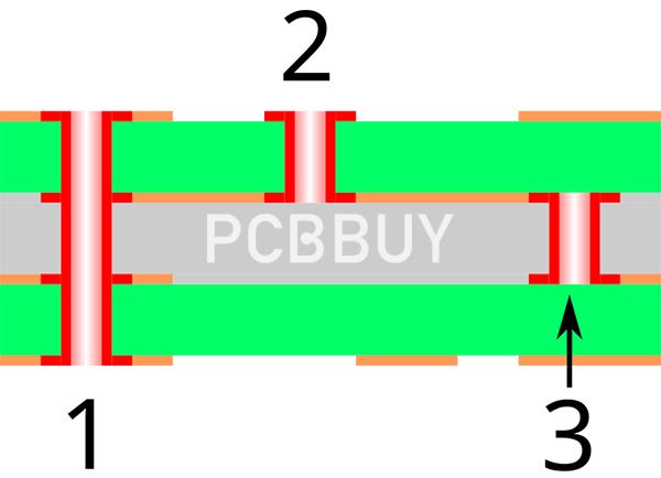
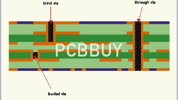
Blind vias connect an outer layer to one or more inner layers without penetrating the entire board.
-
Buried vias connect internal layers only and are completely enclosed within the PCB.
Compared with traditional through holes, these vias provide higher routing density and greater layout flexibility.
|
Via Type |
Connection |
Visible from PCB Surface |
Typical Application |
|
Through Hole Via |
Top to Bottom |
Yes |
Standard multilayer PCB |
|
Blind Via |
Outer Layer to Inner Layer |
One side only |
HDI PCB, smartphones, wearable devices |
|
Buried Via |
Inner Layer to Inner Layer |
No |
High-density multilayer PCB |
|
Microvia |
Laser-drilled blind via |
Usually one layer |
Fine-pitch BGA, AI, 5G, aerospace |
Why Design Optimization Matters?
Blind and buried vias require multiple lamination cycles, laser drilling, precision registration, and advanced plating processes.
Poor design may result in:
-
Low manufacturing yield
-
Misalignment between stacked vias
-
Poor copper plating quality
-
Reliability failures during thermal cycling
-
Increased production cost
-
Signal degradation
-
Reduced assembly reliability
Design optimization ensures the PCB remains manufacturable while meeting electrical and mechanical performance requirements.

Key Design Optimization Techniques
1. Optimize Via Aspect Ratio
The aspect ratio directly affects plating quality.
Recommended practices include:
-
Maintain suitable via depth-to-diameter ratios.
-
Avoid excessively deep blind vias.
-
Follow manufacturer capability guidelines.
Proper aspect ratios improve copper deposition consistency and via reliability.
2. Select Appropriate Via Structures
Different applications require different via configurations.
|
Via Structure |
Advantages |
Recommended Applications |
|
Staggered Microvias |
Lower manufacturing risk |
General HDI products |
|
Stacked Microvias |
Maximum routing density |
Smartphones, AI modules |
|
Blind Via |
Saves routing space |
High-speed digital PCB |
|
Buried Via |
Increases internal routing |
Multilayer industrial PCB |
|
Via-in-Pad |
Short signal path |
Fine-pitch BGA packages |
The optimal structure depends on board complexity, signal requirements, and manufacturing capability.
3. Improve Pad and Capture Pad Design
Proper pad dimensions improve:
-
Registration tolerance
-
Drilling accuracy
-
Copper plating quality
-
Solder joint reliability
Oversized or undersized capture pads can negatively impact manufacturing consistency.
4. Balance Copper Distribution
Uneven copper density around blind and buried vias may cause:
-
Lamination stress
-
Resin flow imbalance
-
PCB warpage
Balanced copper improves:
-
Dimensional stability
-
Lamination quality
-
Via reliability
5. Optimize Layer Stackup
Blind and buried vias are closely related to PCB stackup design.
Well-planned stackups improve:
-
Registration accuracy
-
Controlled impedance
-
Thermal performance
-
Mechanical reliability
PCBBUY provides stackup optimization recommendations during DFM review to support manufacturable HDI designs.
Manufacturing Challenges of Blind and Buried Vias
|
Manufacturing Challenge |
Possible Impact |
Optimization Method |
|
Laser Drilling Accuracy |
Misaligned microvias |
Precision laser drilling equipment |
|
Registration Error |
Via offset |
Tight alignment control |
|
Copper Filling Quality |
Void formation |
Optimized electroplating process |
|
Multiple Lamination Cycles |
Internal stress |
Balanced stackup design |
|
Resin Flow |
Delamination |
Controlled lamination parameters |
|
Aspect Ratio |
Poor plating |
Design within capability limits |
Successful HDI manufacturing requires both optimized design and advanced production processes.
Blind and Buried Via Design for Signal Integrity
Advanced via structures improve electrical performance by:
-
Shortening signal paths
-
Reducing via stub effects
-
Lowering insertion loss
-
Minimizing reflection
-
Supporting high-speed differential routing
These advantages are particularly valuable in:
-
AI servers
-
5G base stations
-
High-speed networking
-
PCIe and DDR memory systems
-
Aerospace electronics
PCBBUY's HDI Manufacturing Capabilities
PCBBUY offers comprehensive HDI PCB manufacturing services designed to support advanced blind and buried via technologies.
|
Capability |
PCBBUY Specification |
|
PCB Layers |
1–26 Layers |
|
HDI Capability |
1st–3rd Order HDI |
|
Blind & Buried Vias |
Supported |
|
Laser Drilling |
High-precision laser drilling |
|
Via Filling |
Resin Filled & Copper Filled |
|
Minimum Mechanical Hole |
0.10 mm |
|
Minimum Line/Space |
35 μm (1.4 mil) |
|
Controlled Impedance |
Single-ended & Differential |
|
Material Options |
FR-4, High-Tg, Rogers, Isola, TUC, Halogen-Free |
|
Quality Inspection |
AOI, Flying Probe Test, X-ray Inspection, Cross-Section Analysis |
|
Engineering Support |
DFM Review, Stackup Optimization, Via Structure Evaluation |
These capabilities enable PCBBUY to manufacture reliable HDI PCBs for demanding applications requiring advanced interconnection technologies.
Design Recommendations Before Manufacturing
Before releasing HDI PCB designs for production, engineers should:
-
Select the most appropriate via structure.
-
Verify aspect ratios with the manufacturer.
-
Optimize pad geometry.
-
Maintain balanced copper distribution.
-
Design symmetrical stackups.
-
Validate impedance requirements.
-
Perform DFM review before fabrication.
-
Confirm manufacturing capability for stacked microvias.
Early collaboration with the PCB manufacturer significantly reduces production risk.
FAQ
Q1: What is the difference between blind vias and buried vias?
Blind vias connect an outer layer to one or more internal layers, while buried vias connect only internal layers and are completely hidden inside the PCB.
Q2: Why are blind and buried vias commonly used in HDI PCBs?
They increase routing density, reduce PCB size, improve signal integrity, and support fine-pitch components such as BGAs.
Q3: Do blind and buried vias increase manufacturing complexity?
Yes. These structures require advanced laser drilling, sequential lamination, precise registration, and specialized plating processes, making them more complex than conventional through-hole vias.
Q4: What factors are most important when optimizing blind and buried via designs?
Critical factors include aspect ratio, stackup design, via structure selection, pad dimensions, copper balance, and manufacturability review.
Q5: How does PCBBUY help optimize blind and buried via designs?
PCBBUY provides comprehensive Design for Manufacturability (DFM) support, including HDI stackup recommendations, via structure evaluation, impedance planning, copper balancing analysis, and engineering optimization before production. Combined with advanced HDI manufacturing equipment and strict quality control, these services help customers achieve reliable, high-yield PCB production.
Conclusion
Effective design optimization for blind and buried vias is essential for producing reliable HDI PCBs that meet the performance demands of modern electronics. By optimizing via structures, stackups, copper balance, and manufacturing parameters, engineers can improve signal integrity, reduce production risks, and enhance long-term product reliability.
With expertise in 1–26 layer PCB fabrication, 1st–3rd order HDI technology, high-precision laser drilling, resin-filled and copper-filled vias, controlled impedance manufacturing, and comprehensive DFM engineering support, PCBBUY delivers advanced PCB manufacturing solutions for customers in AI computing, telecommunications, automotive electronics, industrial automation, aerospace, and other high-performance applications. Its integrated engineering and manufacturing capabilities help transform complex HDI designs into reliable, production-ready circuit boards with consistent quality and performance.
Industry Category








