Design Principles of Inner Layer PCB in Multilayer PCB
By:PCBBUY 01/16/2026 16:04
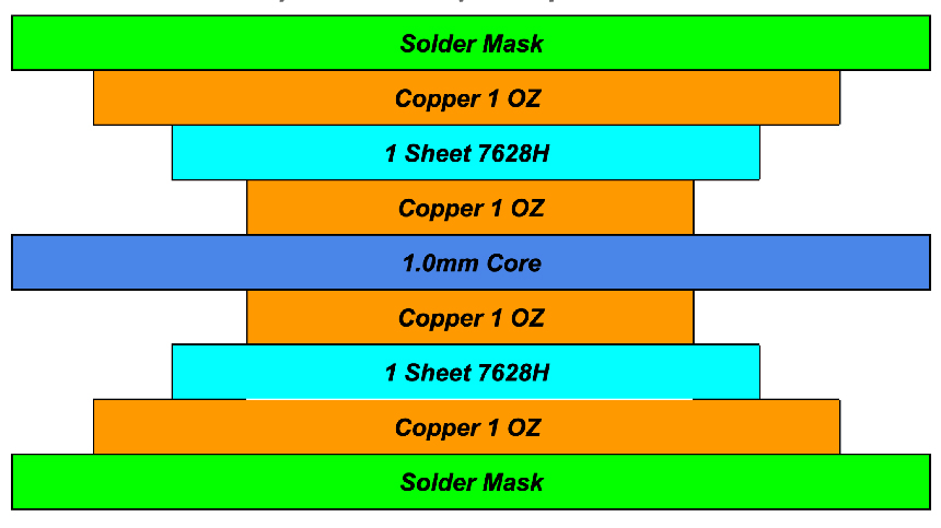
Introduction
In multilayer PCB construction, the inner layer PCB plays a critical role in determining electrical performance, mechanical stability, and overall reliability. Unlike outer layers, inner layers are permanently embedded inside the board after lamination, making defects difficult or impossible to repair. For this reason, inner layer PCB manufacturing requires a high level of process control, precision, and experience.
This article explains what an inner layer PCB is, how it is manufactured, and why inner layer capability is a key indicator of a PCB manufacturer’s technical strength.
What Is an Inner Layer PCB?
An inner layer PCB refers to the copper layers located between the top and bottom surfaces of a multilayer PCB. These layers typically carry:
-
High-speed signal routing
-
Power distribution planes
-
Ground reference planes
Inner layers are formed on copper-clad core materials and later bonded together through lamination to create a multilayer structure.
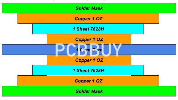
Role of Inner Layers in Multilayer PCB Stackups
Inner layers serve several essential functions:
-
Signal integrity control through controlled impedance routing
-
Power and ground stability via solid copper planes
-
Electromagnetic interference (EMI) reduction
-
Mechanical balance within the PCB stackup
Well-designed and precisely manufactured inner layers ensure consistent electrical performance and long-term reliability.
Materials and Copper Thickness for Inner Layer PCB
Inner layers are typically fabricated using FR-4 core materials, though high-Tg or low-loss materials may be used for advanced applications.
Common inner layer copper thickness options include:
|
Copper Weight |
Typical Thickness |
Application |
|
0.5 oz |
~17 µm |
Fine-line signal layers |
|
1 oz |
~35 µm |
Standard signal and plane layers |
|
2 oz |
~70 µm |
Power distribution and high-current layers |
Selecting the correct copper thickness balances electrical requirements with manufacturability.
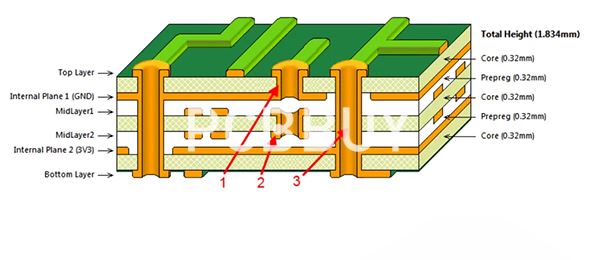
Inner Layer PCB Fabrication Process
1. Inner Layer Imaging
The process begins with photoresist coating and high-resolution imaging to define circuit patterns on the copper surface.
2. Etching
Unwanted copper is removed through controlled chemical etching. Accurate etch compensation is critical to maintain line width and spacing.
3. Resist Stripping and Cleaning
After etching, photoresist is stripped, and the copper surface is thoroughly cleaned.
4. Oxide or Alternative Oxide Treatment
Surface treatment improves copper adhesion during lamination by increasing bonding strength between copper and prepreg resin.
5. Pre-Lamination Inspection
Each inner layer undergoes inspection before lamination to eliminate defects that could be trapped inside the PCB.
Key Manufacturing Challenges of Inner Layer PCB
Manufacturing inner layers involves several technical challenges:
-
Fine line accuracy with tight width and spacing tolerances
-
Copper thickness uniformity across large panels
-
Etching consistency for mixed copper densities
-
Layer-to-layer registration control
Any defect at this stage may result in electrical failure after lamination.

Inner Layer Quality Control and Inspection
Reliable inner layer PCB manufacturing relies on strict quality control:
-
Automated Optical Inspection (AOI) to detect shorts, opens, and pattern defects
-
Dimensional measurement for line width and spacing
-
Process monitoring to ensure etching and imaging stability
Only verified inner layers proceed to the lamination stage.
Lamination Considerations for Inner Layer PCB
During lamination, inner layers are bonded together using prepreg under controlled heat and pressure. Key factors include:
-
Stackup symmetry to prevent board warpage
-
Balanced copper distribution for uniform resin flow
-
Precise alignment to maintain via registration
Strong lamination control ensures electrical continuity and mechanical stability.
Design Guidelines for Inner Layer PCB
To improve manufacturability and reliability, designers should consider:
-
Avoiding extreme copper density differences
-
Maintaining adequate trace width and spacing
-
Using continuous power and ground planes when possible
-
Communicating stackup and impedance requirements early
Early collaboration with the PCB manufacturer helps prevent production risks.
Manufacturing Capability in Inner Layer PCB Production
A manufacturer’s inner layer PCB capability reflects:
-
Precision imaging and etching equipment
-
Stable copper thickness control
-
Advanced lamination and registration processes
-
Comprehensive inner layer inspection systems
These capabilities are essential for complex multilayer PCB fabrication.

Typical Applications of Inner Layer PCB
Inner layer PCBs are widely used in:
-
High-speed digital systems
-
Industrial control electronics
-
Communication and networking equipment
-
Automotive and power electronics
Conclusion
The inner layer PCB is the foundation of multilayer PCB performance and reliability. From imaging and etching to inspection and lamination, each step requires precise control and manufacturing expertise. Strong inner layer capability enables PCB manufacturers to support complex designs, high-layer-count boards, and demanding electrical requirements with confidence.
Industry Category


