EMI PCB Design Guidelines
By:PCBBUY 08/17/2021 17:25

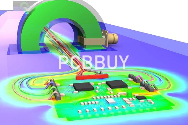
Digital circuits are getting faster and more powerful each year, and as a result, it's more important than ever to utilize proper design techniques and materials to reduce electromagnetic interference (EMI) in our PCB designs. Poor planning can lead to increased and unnecessary radiation, as well as reduced system immunity, which can wreak havoc on our devices.
In this article, we will tell you everything about the EMI PCB design details. Please check and read the content we prepare below for more PCB knowledge. Let’s go!
If you want to order PCB product, please check and custom your order online.
How to optimize EMI PCB Design?
As explained in the previous section, the likelihood that your board or the system on which it operates contains components or equipment that can be classified as radiators is very high. Besides, unless your circuit board is a stand-alone device, the power supply is directly or indirectly connected to the power supply, which is also a common source of electromagnetic interference. The purpose of the EMI filter is to reduce the interference introduced into your board from this source.
EMI filters can be designed from a single component to a complex network with dedicated circuits to mitigate common-mode and different-mode noise. Some basic types of EMI filter design and how to use them are listed below.
Once you have decided on a basic design, it will be necessary to optimize it according to the performance specifications of your circuit and/or board. For example, if your EMI filter is designed to drive other circuits or boards, you may be required to add additional filter elements for isolation, smoothing, or electrical parameter constraints (for example, fixed voltage or current). The extent to which you can meet these circuit requirements depends on the capabilities and capabilities of the PCB design and analysis tools available.
What are the guidelines of EMI PCB design?
As is the case for all circuit board designs, following good EMI filter PCB layout guidelines is essential for manufacturability. Again, the best design requires the adoption of the proper perspective.
2-D PCB Design Perspective
When laying out your board, the first considerations are the locations for component footprints—whether from your design package’s library or uploaded from an external source—trace routing, spacing, or board edge clearance.
· Ensure that pads and component libraries are matched.
· Maximize spacing between adjacent elements—pads, traces, and annular rings—to minimize interference.
· Partition components according to signal types.
· Assure that trace widths and sizes are sufficient for the current capacities required.
· Ensure that impedance matching is instituted where necessary for differential routing, maximum power transfer, etc.
· Follow board clearance rules to facilitate depanelization.
· Use shielding for high radiation devices.
· Make good use of the silkscreen for component polarities and reference indicators to aid assembly.
How to reduce EMI in PCB design?
Ground plane
The ground plane is in many ways your first line of defense against the kind of noise produced by EMI, because circuits require at least a floating ground in order to work. In a PCB board, the ground plane is there to provide a 0 volt reference line to the power supply ground terminal for the return path of a circuit. Unlike the basin, however, when “ripples” are made, noise is produced, dipoles can form and the entire board can become an antenna. This is why the ground plane, that copper foil layer in your PCB, takes up as much of the cross-sectional area of the board as possible. Reducing EMI across your board starts with how effectively you utilize the ground plane.
Trace layout
Traces are conductive paths on a board, which contain flowing electrons while a circuit is active—that means they are just a bend or cross away from creating a fully radiating antenna.
Common best practices for trace layout include:
· Avoid sharp right-angle bends. Capacitance increases in the 45° corner region changing the characteristic impedance and leading to reflections. This can be mitigated by rounding right angles.
· Keep your signals separate. Keep high speed traces (e.g. clock signals) separate from low speed signals, and analog signals separate from digital signals.
· Keep return paths short.
· Route differential traces as close as possible. This increases the coupling factor, bringing influenced noise into the common mode which is less problematic for a differential input stage.
· Use vias wisely. Vias are necessary because they let you take advantage of multiple layers in your boards when routing. Designers must be aware that they add their own inductance and capacitance effects to the mix, and reflections can occur from a change in characteristic impedance.
· Avoid using vias in differential traces. If you must, use an oval anti-pad shared by the two vias to reduce parasitic capacitance.
Industry Category


