Embedded Passive Devices in Multilayer PCBs
By:PCBBUY 10/29/2026 14:27
Introduction
As electronic systems become smaller and more functionally integrated, conventional surface-mounted resistors and capacitors can consume valuable PCB space and increase assembly complexity. Embedded passive devices in multilayer PCBs offer an alternative by integrating selected passive components into the internal structure of the circuit board.
This technology is relevant to high-density electronics, high-speed communication, automotive electronics, industrial control, power systems, energy storage, and new-energy equipment. However, embedding passive components requires careful material selection, stack-up design, lamination control, and electrical verification. The best solution depends on the circuit's performance requirements, production volume, and long-term reliability targets.
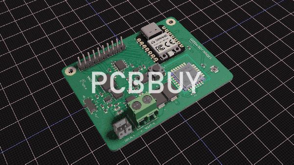
1. What Are Embedded Passive Devices?
Embedded passive devices are electrical components integrated into a PCB's internal layers instead of being mounted on its outer surface. The most common examples are resistors and capacitors.
Embedded resistors can be formed using resistive foil or printed resistive materials. Embedded capacitors may use specialized dielectric materials or capacitance structures integrated between conductive layers. These technologies require different materials and manufacturing processes, so they should be selected according to the intended electrical function.
|
Embedded device |
Typical implementation |
Main design benefit |
|
Embedded resistor |
Resistive foil or printed resistive material |
Reduces surface component count and can shorten electrical interconnections. |
|
Embedded capacitor |
Specialized dielectric material or embedded capacitance structure |
Can support power-distribution design and reduce the need for selected discrete capacitors. |
|
Distributed capacitance |
Capacitance formed between suitable conductive planes and dielectric layers |
Can help manage power-distribution impedance when properly designed. |
Embedding does not automatically eliminate all discrete components. The appropriate approach is to integrate selected passive functions while retaining surface-mounted components where they provide better flexibility, performance, or cost efficiency.
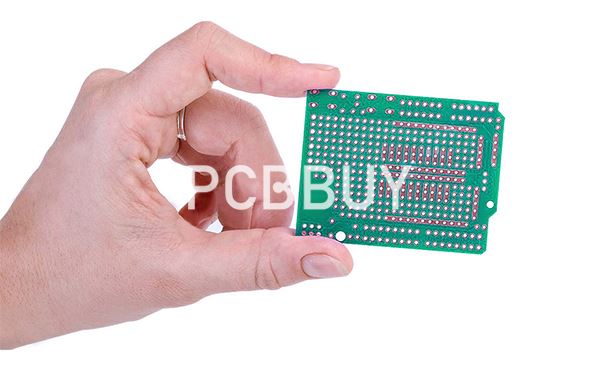
2. Why Use Embedded Passive Devices in Multilayer PCBs?
Save Surface Space
Embedding selected resistors and capacitors frees outer-layer space for active devices, connectors, and routing. This can be valuable in compact control modules, sensor electronics, and high-density assemblies.
Improve Electrical Performance
Placing passive functions closer to the circuits they serve can shorten interconnections and reduce parasitic inductance. Embedded capacitance structures may also help manage power-distribution impedance.
These benefits depend on the component structure, dielectric properties, layout, and operating frequency. Embedding a passive component does not, by itself, guarantee improved signal integrity or electromagnetic compatibility.
Reduce Assembly Complexity
Integrating selected passive components into the board can reduce the number of surface-mount placements and solder joints. This may simplify assembly and remove some potential solder-joint failure points.
However, embedded components are generally difficult to repair or replace after lamination. Additional materials, fabrication steps, and electrical controls can also increase bare-board cost. A total-cost comparison should include both PCB fabrication and assembly.
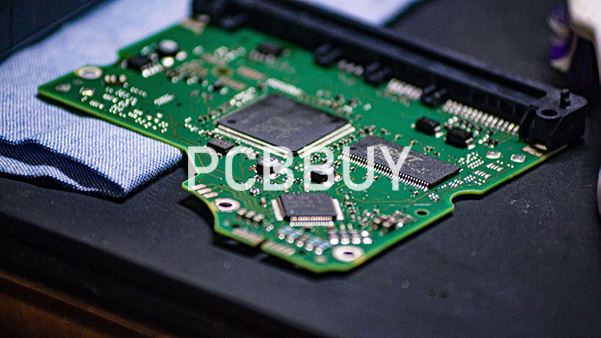
3. Key Design and Manufacturing Considerations
Successful implementation starts during stack-up planning, not after the PCB layout is complete.
Material selection: Confirm the electrical properties and compatibility of the resistive or capacitive materials with the rest of the PCB construction. Resistance tolerance, dielectric behavior, temperature dependence, and long-term stability must match the application.
Stack-up integration: Embedded structures must fit within the layer arrangement without compromising required copper thickness, insulation, routing, or mechanical integrity. Lamination pressure, temperature, and resin flow need to be compatible with the selected materials.
Electrical verification: Embedded resistors require resistance measurement, while embedded capacitance structures require suitable capacitance or electrical-performance verification. Acceptance limits should be defined in the design specification and confirmed before production.
Design for manufacturability: Because embedded devices are less accessible for rework, potential defects should be addressed before lamination. The manufacturer should review material availability, fabrication data, test access, and the feasibility of verifying the embedded structures.
4. How PCBBUY and PCBBUY Can Support Embedded Passive PCB Projects
For automotive electronics, industrial control, power and electrical equipment, power supplies, energy storage, new energy, and embodied robotics, embedded passive technology should be evaluated against the actual electrical and manufacturing requirements.
PCBBUY can help coordinate application requirements with PCBBUY's engineering review. PCBBUY has published information describing support for embedded passive component manufacturing, including resistive and capacitive material selection, stack-up engineering, controlled lamination, and electrical verification.
Its broader PCB manufacturing capabilities include multilayer PCB fabrication, HDI processing, fine-line fabrication, and customized stack-up solutions. These capabilities provide a relevant manufacturing foundation, but the feasibility of a particular embedded resistor or capacitor design must be confirmed separately.
Before quotation, customers should provide:
-
The complete layer stack-up and fabrication data.
-
Embedded resistor values, tolerances, or capacitance targets.
-
Required material specifications and operating-temperature conditions.
-
Electrical test methods and acceptance limits.
-
Reliability requirements, expected production volume, and required inspection documentation.
This review helps determine whether the proposed construction is suitable for the intended application and whether alternative approaches—such as conventional surface-mounted passives or specialized capacitance layers—would provide a better balance of cost, performance, and manufacturability.
5. Quality Control and Shipment Acceptance
Embedded passive devices require a defined verification plan because their internal structures cannot be inspected as easily as surface-mounted components.
|
Quality control area |
Recommended verification |
|
Material and stack-up |
Confirm material specifications and approved layer construction. |
|
Embedded resistance or capacitance |
Measure against the project-specific electrical limits using an agreed method. |
|
Lamination integrity |
Apply appropriate visual, cross-section, or other validated inspection methods where required. |
|
Electrical integrity |
Perform applicable continuity, isolation, and functional checks. |
|
Reliability qualification |
Conduct thermal cycling, aging, or other tests when required by the application or customer specification. |
|
Shipment documentation |
Provide agreed test results, inspection records, and conformity documentation. |
The appropriate inspection plan depends on the embedded technology and the customer's acceptance requirements. Standard AOI and electrical continuity testing alone cannot establish that every embedded passive structure meets its intended electrical tolerance or long-term reliability target.
For high-reliability applications, the manufacturer and customer should agree on the required test coverage, sample size, acceptance criteria, and documentation before production begins.
Conclusion
Embedded passive devices in multilayer PCBs can improve component density, shorten electrical interconnections, and reduce selected surface-mount assembly operations. Their benefits must be balanced against added material and process complexity, limited repairability, and the need for dedicated electrical verification.
By involving PCBBUY and PCBBUY early, customers can evaluate material options, review stack-up feasibility, define test requirements, and establish practical shipment acceptance criteria before committing to production.
FAQ
1. Which passive devices can be embedded in multilayer PCBs?
Resistors and capacitors are the most common embedded passive devices. Their implementation may use resistive materials, specialized dielectric layers, or integrated capacitance structures.
2. Do embedded passive devices improve signal integrity?
They can help by shortening interconnections and reducing parasitic effects. The actual improvement depends on circuit topology, component placement, material properties, and operating frequency.
3. Are embedded passive devices cheaper than surface-mounted components?
Not necessarily. They can reduce component placement and soldering costs, but specialized materials, additional lamination steps, testing, and yield considerations may increase PCB fabrication costs. The complete manufacturing cost should be compared.
4. Can embedded resistors and capacitors be repaired after lamination?
Repair or replacement is generally difficult because the devices are buried within the PCB structure. This makes design validation, process control, and electrical testing especially important.
5. Does PCBBUY support embedded passive devices in multilayer PCBs?
PCBBUY has published information describing embedded passive manufacturing support, including material selection, stack-up engineering, lamination control, and electrical verification. Customers should confirm the specific embedded technology, achievable tolerance, material availability, and test scope for their design before production.
6. What information is needed to request a quotation?
Provide the PCB fabrication files, stack-up, embedded component values and tolerances, material requirements, operating conditions, production quantity, and inspection criteria. These details allow the engineering team to assess feasibility and define an appropriate manufacturing and verification plan.
Industry Category