Full Guide to ENEPIG Process in PCB Manufacturing
By:PCBBUY 07/25/2025 14:01
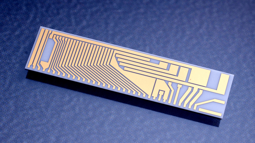
In the fast-evolving world of PCB technology, surface finish quality plays a pivotal role in determining the reliability, bondability, and solderability of electronic circuits. Among the various surface finish methods, the ENEPIG process (Electroless Nickel Electroless Palladium Immersion Gold) stands out as the premium solution for high-performance applications. At PCBBUY, we have perfected the ENEPIG process through years of technical refinement, strict tolerance control, and material excellence.
1. What Is the ENEPIG Process?
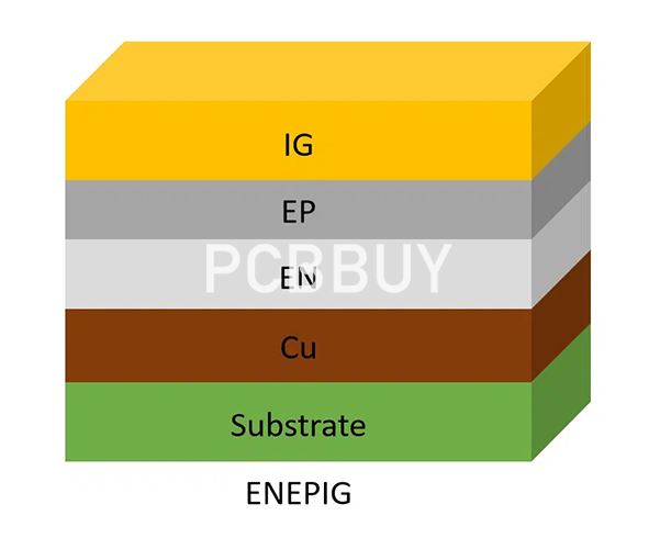
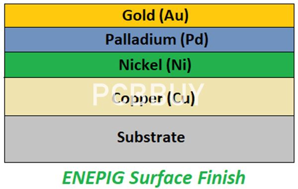
The ENEPIG process is a multi-layer metal coating technique applied to printed circuit boards (PCBs) to ensure robust electrical performance and long-term corrosion resistance. It involves three key plating steps:
-
Electroless Nickel (Ni): Provides barrier protection and serves as the foundation layer.
-
Electroless Palladium (Pd): Prevents nickel diffusion and improves wire bondability.
-
Immersion Gold (Au): Offers excellent surface conductivity and oxidation resistance.
Each of these layers contributes to the mechanical stability and electrical performance of modern PCB assemblies, especially those requiring wire bonding, fine-pitch components, and BGA pads.
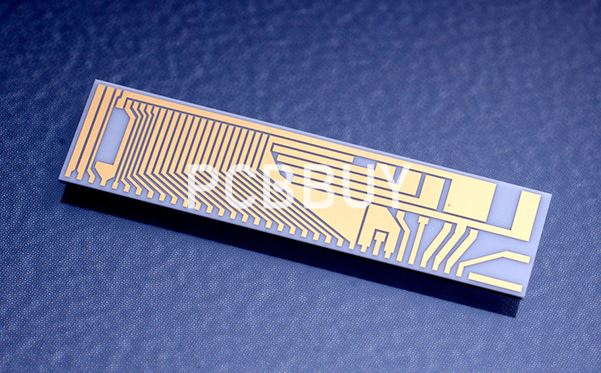
2. The ENEPIG Process Workflow at PCBBUY
At PCBBUY, our ENEPIG process follows a controlled, automated sequence to ensure uniformity and repeatability across large volumes.
a. Copper Surface Cleaning & Activation
-
Microetching and pre-cleaning the copper pad to enhance adhesion
-
Chemical activation of the copper layer for consistent deposition
b. Electroless Nickel Plating
-
Standard thickness: 200µ”
-
Ensures excellent solder joint integrity and prevents copper diffusion
c. Electroless Palladium Deposition
-
Thickness range: 1–10µ”
-
Key to preventing nickel corrosion (“black pad”)
-
Essential for gold wire bonding and high-reliability interconnects
d. Immersion Gold Plating
-
Thickness range: 1–10µ”
-
Provides oxidation protection and a flat surface for soldering and bonding
All plating steps are continuously monitored using XRF thickness measurement systems and supported by automated dosing controllers to maintain precise chemical balance.
3. PCBBUY’s ENEPIG Process Specifications and Customization
|
Metal Layer |
Standard Thickness |
Customization Capability |
|
Nickel (Ni) |
200µ” |
Up to 300µ” max |
|
Palladium (Pd) |
1–10µ” |
≤30µ” total (Pd+Au) |
|
Gold (Au) |
1–10µ” |
≤30µ” total (Pd+Au) |
Note: Special ENEPIG process thickness specifications can be customized to meet specific wire bonding, soldering, or shelf-life requirements.
4. Advantages of the ENEPIG Process in PCB Applications
Choosing the ENEPIG process provides numerous benefits, particularly in high-end electronic systems:
-
✅ Excellent solderability and wetting performance
-
✅ Superior gold and aluminum wire bond compatibility
-
✅ No black pad effect (unlike ENIG)
-
✅ High resistance to corrosion and oxidation
-
✅ Stable under multiple thermal cycles
-
✅ Ideal for BGA, QFN, COB, and high-frequency PCBs
5. ENEPIG Process vs Other PCB Surface Finishes
|
Property |
ENEPIG |
ENIG |
HASL |
OSP |
|
Wire bondability |
✅ Excellent |
❌ Limited |
❌ No |
❌ No |
|
Surface flatness |
✅ Very High |
✅ High |
❌ Low |
✅ High |
|
Cost |
💲💲💲 |
💲💲 |
💲 |
💲 |
|
Solder joint reliability |
✅ High |
✅ Medium |
❌ Low |
✅ Medium |
ENEPIG offers the best overall balance of performance, bondability, and reliability, making it the surface finish of choice for precision-driven industries.

6. Application Fields That Rely on the ENEPIG Process
PCBBUY’s ENEPIG-finished PCBs are widely adopted across:
-
Aerospace and military electronics
-
High-speed computing modules
-
Medical imaging and diagnostic systems
-
Automotive radar and safety circuits (ADAS)
-
Semiconductor testing and wafer-level packaging
7. Why Choose PCBBUY for ENEPIG PCBs?
-
🌐 Global-standard process lines built for precision multilayer boards
-
🔬 Full in-line process control for Ni/Pd/Au uniformity
-
🧪 Material sourcing from top-tier suppliers (e.g., Rohm & Haas, Uyemura)
-
📦 Flexible production from prototype to mass production
-
🛠️ Engineering support for ENEPIG + via-in-pad or HDI designs
8. Frequently Asked Questions About the ENEPIG Process
Q: Can I request special thickness combinations of Pd and Au?
A: Yes. PCBBUY allows customization of the ENEPIG process with Pd/Au combinations up to a total of 30µ”, based on application needs.
Q: Is the ENEPIG process suitable for fine-pitch BGA?
A: Absolutely. The ENEPIG surface provides excellent coplanarity and oxidation resistance for ultra-fine-pitch devices.
Q: How does PCBBUY control black pad in the ENEPIG process?
A: Our electroless nickel and palladium plating baths are optimized with real-time analytics to avoid corrosion-prone conditions that lead to black pad.
Conclusion
As miniaturization and performance demands increase across industries, the ENEPIG process is becoming the go-to finish for designers who prioritize bondability, durability, and long-term reliability. At PCBBUY, we continuously optimize our ENEPIG capabilities to deliver high-performance PCB solutions at competitive costs.
Contact PCBBUY today for a custom ENEPIG quote or free DFM review of your PCB design.
Industry Category


