Gold Fingers PCB and Advanced Manufacturing Capabilities
By:PCBBUY 08/19/2025 14:37

Introduction to Gold Fingers PCB
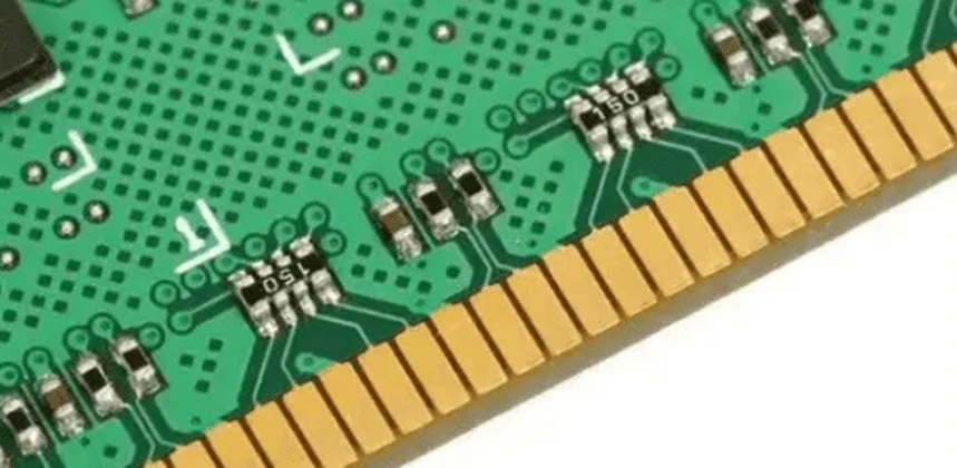
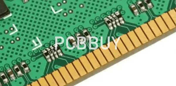
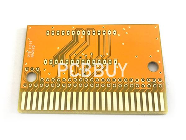
In modern electronic design, Gold Fingers PCB has become an essential solution for ensuring reliable connectivity between circuit boards and electronic modules. Gold Fingers refer to the gold-plated connectors located on the edge of a PCB, designed to withstand repeated insertion and removal cycles. They provide excellent electrical conductivity, corrosion resistance, and mechanical durability, making them indispensable in high-performance electronics such as memory modules, graphics cards, industrial controllers, and communication devices.
At PCBBUY, we specialize in advanced Gold Fingers PCB manufacturing, offering high-precision selective electroplating, customized plating thickness, and international quality assurance.
Structure and Function of Gold Fingers in PCB
A Gold Fingers PCB is designed with edge connectors plated with a thin layer of gold to enhance signal integrity and extend product lifespan.
-
Signal Transmission: Ensures stable high-frequency signals without interference.
-
Durability: Gold plating resists oxidation and supports thousands of insertion cycles.
-
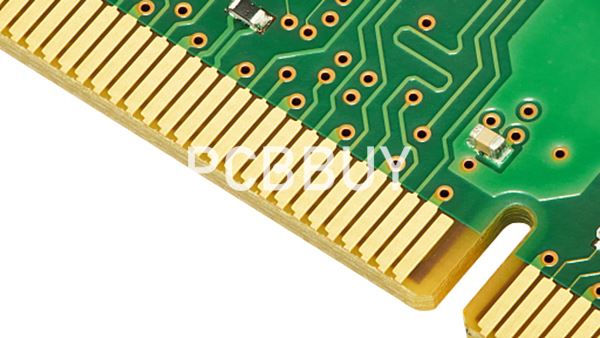
Mechanical Precision: Chamfered edges allow smooth insertion into connectors without damaging pads.
Applications include computer motherboards, RAM modules, GPUs, networking equipment, and plug-in industrial automation systems.

PCBBUY’s Gold Fingers PCB Manufacturing Capabilities
PCBBUY integrates world-class plating technology and strict quality standards to deliver high-reliability Gold Fingers PCB solutions.
-
Selective Electroplating + Gold Fingers: Advanced process ensures gold is deposited only on connector edges, saving material cost while ensuring high performance.
-
Gold Thickness Range: AU plating thickness from 3 μin to 100 μin is available, meeting diverse requirements from consumer electronics to industrial-grade PCBs.
-
Lead Options: Customers can choose residue or non-residue selective leads when placing an order, ensuring compatibility with different assembly environments.
-
Chamfering (Beveling) Process: Guarantees smooth insertion into connectors and minimizes wear.
-
Surface Treatment: Flat, burr-free edges for reliable connections.
This flexibility allows PCBBUY to supply both standard and customized Gold Fingers PCB solutions for global clients.

Gold Fingers PCB Manufacturing Process at PCBBUY
The production of Gold Fingers PCB involves multiple precision steps:
-
Base Material Preparation – High-quality FR4 or advanced laminates ensure dimensional stability.
-
Nickel Plating Layer – A nickel barrier layer is electroplated to provide adhesion for gold and prevent copper migration.
-
Gold Electroplating – Selective hard gold or soft gold plating is applied, with thickness ranging from 3–100 μin depending on customer requirements.
-
Chamfering and Polishing – Connector edges are chamfered (typically 30° or 45°) for smooth module insertion.
-
Surface Cleaning – Removes contaminants and ensures a flawless finish.
-
AOI & Electrical Testing – 100% visual inspection and signal integrity testing ensure compliance with IPC-Class 2/3 standards.

Quality Control in Gold Fingers PCB Production
At PCBBUY, strict quality control is at the core of Gold Fingers PCB production:
-
Plating Thickness Measurement – Ensures precise Au thickness (3–100 μin).
-
Appearance Inspection – Detects scratches, oxidation, or burrs.
-
Insertion and Durability Testing – Simulates thousands of plug-in cycles to verify mechanical stability.
-
Impedance and Conductivity Tests – Guarantee reliable electrical performance.
-
Compliance – Meets IPC,UL, and RoHS international certifications, making PCBBUY products suitable for global export.
Applications of Gold Fingers PCB
Gold Fingers PCBs are widely used in:
-
Computing Hardware – RAM, graphics cards, motherboards.
-
Industrial Control Systems – Modular plug-in boards.
-
Networking Equipment – Routers, switches, and communication devices.
-
Consumer Electronics – Devices requiring reliable edge connections.
Why Choose PCBBUY for Gold Fingers PCB
PCBBUY is a trusted Gold Fingers PCB manufacturer with advanced technology and a strong export background:
-
Precision Equipment: Uniform gold plating, controlled chamfering, and automated inspection.
-
Customizable Solutions: Adjustable Au thickness and selective electroplating for different industries.
-
International Standards: Compliance with IPC, ISO, and RoHS ensures reliable quality.
-
Flexible Production: Supports both prototype and mass production.
-
Global Experience: Years of OEM/ODM cooperation with international clients.
Conclusion
Gold Fingers PCB technology is crucial for reliable and long-lasting electronic interconnections. With advanced selective electroplating, customizable plating thickness, and strict international testing standards, PCBBUY delivers premium Gold Fingers PCB manufacturing solutions trusted by global customers.
If you are looking for a professional supplier to support your projects with high-quality Gold Fingers PCB, contact PCBBUY today for consultation and a free quotation.
Industry Category


