HDI PCB Design Guide: Advanced Manufacturing Capabilities
By:PCBBUY 06/11/2025 15:14
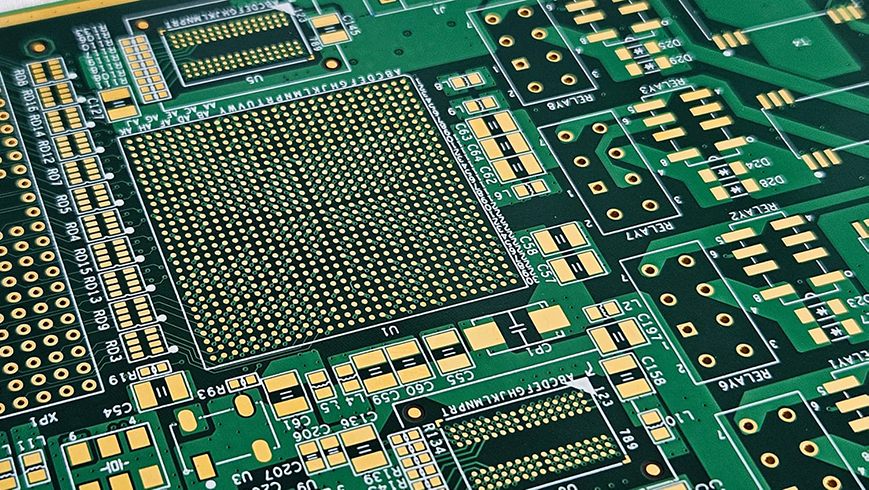
In the ever-evolving world of electronics, High-Density Interconnect (HDI) PCBs play a pivotal role in driving miniaturization, performance, and integration. At PCBBUY, our manufacturing processes are designed to meet the highest standards of precision and efficiency. This HDI PCB design guide aims to walk you through our advanced capabilities, offering technical insights for engineers, designers, and procurement professionals.
How to Choose Advanced Material in HDI PCB Design Guide?
In high-density interconnect (HDI) PCB design, material selection plays a critical role in thermal stability, signal integrity, and mechanical reliability. At PCBBUY, we primarily utilize FR-4 base materials with customizable TG (glass transition temperature) ratings, including TG135 to TG170, as well as halogen-free and high CTI (Comparative Tracking Index) substrates upon request.
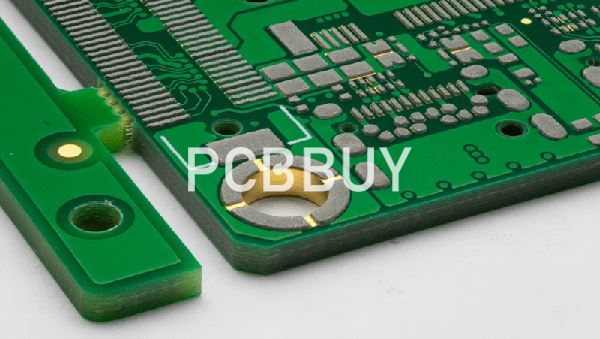
High-TG materials are especially recommended for multi-layered HDI boards subjected to lead-free soldering or operating under high ambient temperatures. For example:
|
Material Type |
TG Value (°C) |
CTI Rating |
Application Example |
|
FR-4 (Standard) |
135°C |
≥175V |
General-purpose consumer electronics |
|
FR-4 (High TG) |
170°C |
≥300V |
Automotive control systems |
|
Halogen-Free FR4 |
150-170°C |
≥600V |
Green-compliant medical devices |
Layer Structure in HDI PCB Design Guide
The core of HDI PCB design lies in the construction order and layer stacking. PCBBUY supports 1+N+1 to 2+N+2 constructions, with capabilities extending to 10+ layer advanced HDI for complex system-on-board applications.
Typical configurations include:
-
1+N+1: Basic HDI with a single microvia layer on both outer layers.
-
2+N+2: Advanced configuration allowing two sequential lamination cycles.
-
Any Layer HDI: All layers can connect with laser vias, enabling maximum design flexibility.
Blind vias are implemented with either laser or mechanical drilling:
|
Via Type |
Min Hole Diameter |
Method |
Copper Thickness |
|
Laser Blind Via |
≥0.075 mm |
Laser |
≥13 μm |
|
Mechanical Via |
≥0.15 mm |
Mechanical |
≥18 μm (no laser) |
PCBBUY ensures full via metallization through electroplated copper filling, meeting IPC-6012 Class 2 or 3 standards with via fill depth tolerance of ±15%.
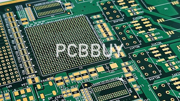
Trace Width and Hole Size of HDI PCB Design Guide
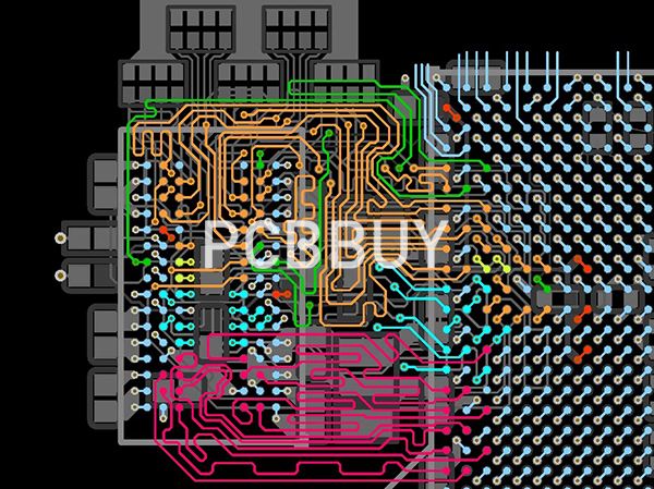
Signal routing is another key focus in HDI PCB design. PCBBUY supports a minimum trace width and spacing of 2/2 mil, critical for high-speed differential pair designs such as LVDS, USB 3.1, and PCIe.
In addition, PCBBUY's advanced laser drilling and image transfer processes allow for:
-
Hole size minimum: 0.075 mm (laser) / 0.15 mm (mechanical)
-
Minimum pad size: 0.15 mm
-
Aspect ratio for vias: Up to 1:1 for blind vias
-
Drill to copper clearance: As low as 100 μm
These capabilities help customers meet the increasing demand for miniaturized, high-frequency circuits in mobile, medical, and RF applications.
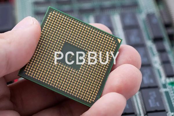
Copper Plating and Via Filling of HDI PCB Design Guide
One of the most common reliability risks in HDI PCBs is incomplete via metallization. At PCBBUY, we adopt laser via electroplating with controllable depth (0.05 mm–0.1 mm), ensuring excellent conductivity and mechanical robustness.
Key specs include:
-
Laser via copper thickness: ≥13 μm (typical), customized upon request.
-
Via copper fill ratio: ≥95% for critical net vias.
-
Electroplating uniformity: ±10% within the same panel area.
Additionally, plugged and capped via processes are offered for solder mask coverage and SMT land finish integrity.
DFM Integration in HDI PCB Design Guide
PCBBUY provides full-stack Design for Manufacturability (DFM) feedback to ensure customers' HDI designs are fully optimized for volume production.
Our DFM services include:
-
Gerber/ODB++ layer analysis for microvia and pad alignment.
-
Impedance modeling with stack-up proposal.
-
Blind/buried via structure validation with lamination sequence.
-
BOM and stencil review for surface assembly readiness.
PCBBUY utilizes AOI, flying probe testing, X-ray via inspection, and cross-section analysis to validate critical parameters per IPC-A-600 Class 2/3.
HDI Applications Enabled by PCBBUY's Capabilities
Our HDI solutions have been successfully deployed across numerous industries:
|
Industry |
Typical Stack-Up |
Key Features |
|
Wearable Devices |
1+6+1 |
Ultra-thin board, laser vias, 2 mil spacing |
|
Automotive Radar |
2+8+2 |
High Tg, impedance control, EMC shielding |
|
Industrial IoT |
Any-Layer (10L) |
Blind & buried vias, EMI filter integration |
We also support special requirements like ENIG, OSP, immersion silver, and carbon ink printing for contact switches or keyboard modules.
Conclusion: Why Choose PCBBUY for HDI PCB Manufacturing?
Our strength lies in our commitment to precision, customization, and scalable HDI production. With a robust QA system and advanced production lines, PCBBUY can meet the demands of the most intricate HDI PCB designs.
✔️ Benefits of choosing PCBBUY:
-
Full support for multi-stage HDI structures
-
Laser via drilling and filling capabilities
-
Customizable materials and stack-ups
-
Tight trace/space resolution with AOI and LDI support
-
Engineering review and one-on-one DFM support
Get a Quote Today
If you're working on a project that requires advanced HDI PCB manufacturing, we encourage you to contact PCBBUY for a free quote. Our engineers are ready to assist you from design to delivery.
Industry Category


