HDI PCB Fabrication Capabilities: Advanced Technology
By:PCBBUY 06/11/2025 15:49
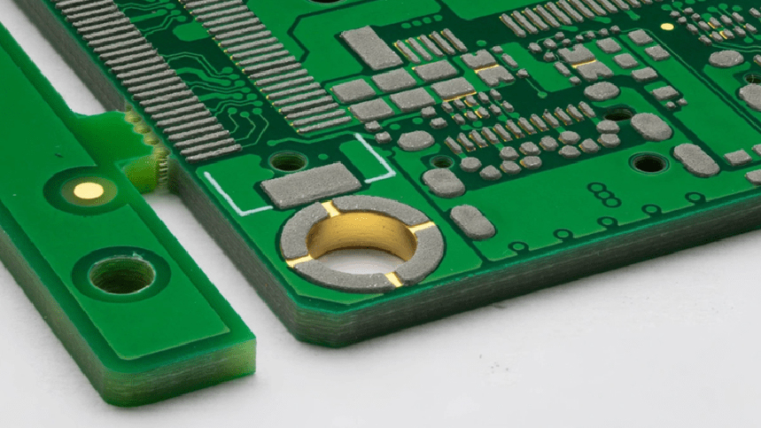
As high-performance, miniaturized electronics dominate the market, HDI PCB fabrication (High-Density Interconnect Printed Circuit Board fabrication) is at the forefront of advanced electronic design. At PCBBUY, we offer industry-leading HDI PCB manufacturing services—from prototype to mass production—backed by precision equipment, expert engineering, and a commitment to quality.
This article introduces our full range of HDI PCB fabrication capabilities, including technical standards, process highlights, and material options. Whether you’re developing wearable technology, communication modules, or automotive sensors, PCBBUY’s HDI production line delivers reliability, precision, and scalability.
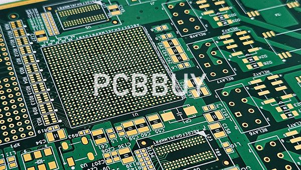
1. HDI PCB Fabrication Materials and Layering Options
● Material Options
|
Our default HDI PCB material is high-quality FR-4, with customizable thermal and environmental performance. We support TG135–TG170 and halogen-free materials as well as CTI-rated ItemStandardRemarksMaterialFR-4TG135–TG170, halogen-free / CTI materials can be customized |
● Layer Capabilities
-
1st-order HDI: 4–10 layers
-
2nd-order HDI: 6–10 layers
Layer stack-up customization is available based on application needs.
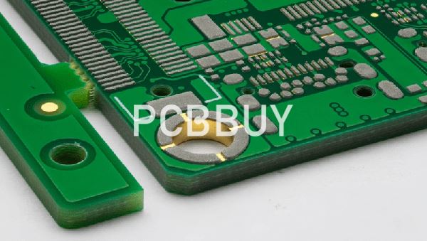
2. Construction Types for HDI PCB Fabrication
We support a wide variety of sequential lamination structures including:
-
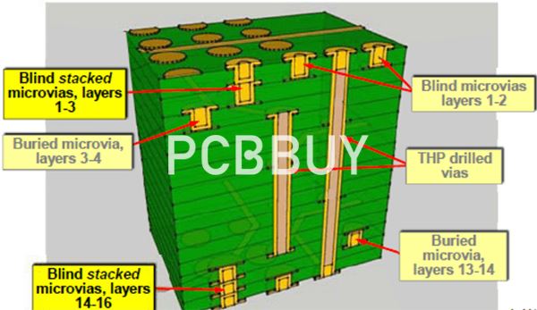
1st order: 1+N+1, 1+1+N+1+1
-
2nd order: 2+N+2, 1+2+N+2+1
These support buried vias ≤ 0.3 mm, with mechanical or laser drilled microvias. Based on your Gerber stack-up or design file, our team will choose the most efficient method—mechanical drill or electroplating via filling process.
3. Precision Trace Width in HDI PCB Fabrication
PCBBUY maintains minimum trace width/spacing of 2/2 mil, ideal for high-density, high-frequency boards used in RF or digital signal processing.
This fine resolution is supported by advanced dry-film imaging and AOI (Automated Optical Inspection) systems to ensure signal integrity and impedance control.
4. Advanced Blind Via and Microvia Technology
We support both mechanical and laser-drilled blind vias:
-
Mechanical blind via: ≥0.15 mm
-
Laser blind via: ≥0.075 mm
This provides flexibility based on cost and performance requirements. For multi-stack structures, we offer stacked or staggered via architectures.
5. HDI PCB Fabrication Drill Hole Size and Copper Requirements
Our standard via hole size tolerance and hole copper plating ensure robustness during assembly and repeated thermal cycles.
|
Item |
Standard |
Remarks |
|
Hole Size |
Minimum unilateral ≥ 3 mil |
May be adjusted |
|
Hole Copper |
>18 µm (no laser via), >13 µm (laser via) |
Verified via cross-section inspection |
6. Via Filling and Electroplating Control in HDI PCB Fabrication
PCBBUY uses advanced laser via electroplating technology to ensure 100% metallization:
-
Filling depth: 0.05–0.1 mm
-
Tolerance: ±15%
The hole is filled with copper to ensure smooth pad formation and excellent BGA solderability.
7. End-to-End HDI PCB Fabrication Workflow at PCBBUY
● Design Verification & CAM Optimization
We verify all customer stack-up and drill data, optimizing for impedance, thermals, and manufacturability.
● Laser Microvia Drilling & X-ray Positioning
High-accuracy UV laser systems drill sub-100µm vias with automated X-ray alignment for perfect layer registration.
● Sequential Lamination
Multilayer builds such as 2+N+2 use high-Tg resin systems and low CTE (Coefficient of Thermal Expansion) to maintain dimensional stability.
● Via Filling & Electroplating
Full-fill plating of blind vias ensures no air gaps, eliminating potential failure points during BGA soldering or reflow.
● Surface Finishes
We offer ENIG, immersion silver, OSP, and ENEPIG compatible with HDI stack-ups.
Conclusion: Why Choose PCBBUY for HDI PCB Fabrication
At PCBBUY, we combine engineering expertise with scalable infrastructure to meet all levels of HDI PCB fabrication—from quick-turn prototypes to volume production. Our deep capabilities in microvia control, fine line etching, laser drilling, and via plating allow us to serve high-end industries like medical, aerospace, and telecommunications.
If you’re looking for a professional HDI PCB manufacturer with custom stack-up solutions, tight tolerance control, and fast lead times, PCBBUY is your trusted partner.
Industry Category


