HDI PCB Stackup Capabilities for High-Density Applications
By:PCBBUY 06/19/2025 14:34
In the fast-evolving world of electronics, HDI (High-Density Interconnect) PCBs have become a critical component for compact, high-performance devices. At PCBBUY, a leading HDI PCB stackup manufacturer in China, we deliver engineered stackup solutions that ensure signal integrity, miniaturization, and robust mechanical reliability. This article explores our HDI PCB stackup capabilities based on industry standards and our proprietary manufacturing process.
1. What Is HDI PCB Stackup and Why It Matters
An HDI PCB stackup refers to the layer configuration and interconnection structure in a high-density circuit board. Proper stackup design is crucial for high-speed signal performance, thermal management, and compact layout.
At PCBBUY, we provide 1st-order stackups (1+N+1) and complex multi-order stackups (2+N+2, 3+N+3, etc.), accommodating the most demanding HDI designs across multiple industries, including mobile, automotive, and medical devices.

2. PCBBUY's HDI PCB Stackup Capabilities
|
Item |
Specification |
|
Material |
FR-4 base, TG135-TG170, halogen-free and CTI-customizable materials |
|
Number of Layers |
1st order: 4-10 layers; 2nd stage: 6-10 layers |
|
Construction Types |
1+N+1, 1+1+N+1+1; 2+N+2, 1+2+N+2+1 (n buried vias ≤ 0.3mm) |
|
Trace Width |
Minimum 2/2mil (50µm/50µm) |
|
Blind Vias |
Mechanical: ≥0.15mm; Laser: ≥0.075mm |
|
Hole Size |
Minimum unilateral ≥3mil (75µm) |
|
Hole Copper |
≥18µm for no laser burial; ≥13µm for laser buried vias |
|
Via Electroplating |
0.05mm–0.1mm depth with ±15% tolerance |
Our stackup engineering focuses on signal layer placement, via optimization, and copper balancing to enhance EMC, impedance control, and manufacturability.
3. Advanced Construction Types for Complex HDI PCB Stackups
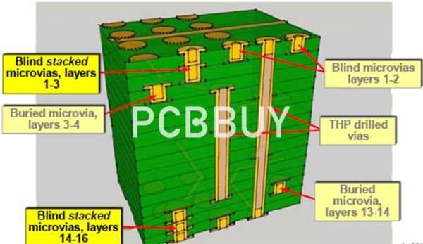
PCBBUY supports single, double, and multiple HDI stackup configurations. Popular examples include:
-
1+N+1: A single build-up layer on both sides of the core.
-
2+N+2: Two build-up layers for higher routing density.
-
Any-layer HDI: Fully interconnected layers using laser vias for ultra-high-density devices.
We prioritize internal mechanical via structures based on customers' laminated stackup drawings. When needed, we implement via filling and copper plating processes for enhanced structural stability.
4. Key Processes Behind Our HDI Stackup Manufacturing
-
Laser Drilling: Precision laser drilling enables blind vias as small as 0.075mm.
-
Sequential Lamination: Multistage lamination for multi-order stackups.
-
Via Filling & Electroplating: Copper is filled into via holes to ensure full metalization.
-
Impedance Control: Adjusted dielectric thickness and trace geometry to maintain tight signal performance.
All stackups undergo thorough design review, including thermal expansion simulation and manufacturability assessments.

5. Customized Materials and Quality Control
We offer flexible options including:
-
Base Materials: FR-4, TG135-TG170, halogen-free, or CTI-rated options
-
Custom Trace Widths: Starting from 2mil for high-density routing
-
Electroplating Tolerance: Maintained within ±15% to ensure reliable conductivity
Our in-house engineering team works closely with clients to evaluate via reliability, copper thickness uniformity, and stackup impedance.

6. Why PCBBUY for Your HDI PCB Stackup Needs
-
Strong R&D support for multi-order stackups
-
Competitive lead times and scalable volume production
-
Engineering assistance with stackup review and optimization
-
Fully customized stackup proposals based on your Gerber or stackup design
7. FAQ: 5 Common Questions About HDI PCB Stackup
Q1: What is the best stackup type for signal integrity in HDI PCBs?
A: A symmetrical stackup with controlled impedance layers is preferred, such as 1+N+1 or 2+N+2, depending on signal speed and density.
Q2: Can I customize the dielectric material in the stackup?
A: Yes, PCBBUY offers FR-4, high-Tg, halogen-free, and CTI-custom materials to meet electrical and environmental demands.
Q3: What’s the minimum via size PCBBUY can support?
A: For laser vias, the minimum hole size is 0.075mm; for mechanical blind vias, it’s 0.15mm.
Q4: How do you ensure copper consistency in via filling?
A: We use laser via electroplating with copper fill, ensuring complete metalization and depth tolerance within ±15%.
Q5: Does PCBBUY support stackup design assistance?
A: Absolutely. Our engineering team offers DFM reviews, stackup simulations, and structure recommendations based on your application.
Industry Category


