HDI PCB design guidelines
By:PCBBUY 08/09/2021 17:29

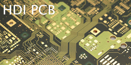
High density interconnects (HDI) layout refers to a set of techniques used to layout a PCB when traces widths generally drop below 8 mils (0.2 mm). These techniques are designed to ensure you can fit a higher density of components onto a single board, allowing you to keep your board size small while increasing component count. Not all boards need HDI layout techniques for a number of reasons, while some components require HDI techniques for proper routing.

What are the features of HDI PCB design?
An HDI board requires smaller vias to make layer transitions, particularly in fine-pitch BGA components and more traces per sq. mm. In order to accommodate fine-pitch components, you'll find the following typical features in an HDI layout:
Smaller vias: HDI boards use microvias (mechanically or laser drilled), blind/buried, and staggered vias for layer transitions. These vias have smaller aspect ratios than typical through-hole vias. In order to use these vias with finer pitch components, their diameters are smaller, which then limits their useful depth.
Thinner traces: The thinner traces used in HDI boards are required to make connections to vias on each layer, as well as to in-pad vias. The thinner traces also allow higher trace density, thus the term HDI. Higher layer count: We've built non-HDI boards with high layer counts, but HDI board layer counts can easily reach 20 or more layers when working with high pin density components (e.g., FPGAs).
Lower signal levels: HDI boards are not used for high voltage or high current. This is because the high field strength between neighboring lines will cause ESD, and high currents will cause excessive temperature rise in conductors.
What are the technologies of HDI PCB design?
The difficulties of HDI PCB fabrication lie in micro-via fabrication, via metallization and fine lines.

1. Micro-via fabrication
Micro-via fabrication has always been the core problem in HDI PCB manufacturing. There are two main drilling methods:
1). As for ordinary via drilling, mechanical drilling is always the best choice for its high efficiency and low cost. With the development of mechanical processing capacity, its application in micro-via has been on the way as well.
2). There are two types of laser drilling: photothermal ablation and photochemistry ablation. The former refers to the process during which the operated material is heated to be melted after absorbing laser with high energy and is evaporated off with via formed. The latter refers to the result caused by high-energy photons in UV zone and with laser length more than 400nm.
2. Via metallization
The biggest difficulty for via metallization is it is difficult for plating to reach uniform. As for the deep-hole plating technology for micro-via, besides the usage of plating solution with high dispersing power, via plating solution on plating devices should be upgraded in time that can be accomplished by either strong mechanical stirring or vibration, ultrasonic stirring, horizontal spraying. Also, the humidity of via wall must be increased before plating.
3. Fine lines
The implementations of fine lines include traditional image transfer and laser direct imaging. Traditional image transfer has the same process with the ordinary chemical etching to form lines.
As for laser direct imaging, photographic film isn't needed while images are formed directly on photosensory membrane through lasers. UV wave light is used to operate so that liquid anti-corrosion solution is capable of meeting demands of high resolution and simple operation.
What are the basic HDI PCB design guidelines?
When working with fine-pitch BGA, and the traces and vias that connect to it, there are some basic guidelines that apply to any HDI layout.

1. Always check your manufacturer's capabilities. You should generally do this anyways before planning a new design, but nowhere else is this more important than in HDI design. Not all manufacturers have the same capabilities in this area, and it's best to check with your desired manufacturer before you create an HDI layout that can't be fabricated.
2. Keep track of spacing between traces and pads. The same idea applies in 1 mm pitch BGAs, the only point that changes is scaling to microvia sizes. Solder mask clearance values are typically on the same size as your trace width. The solder mask clearance depends on the pad size and your pad pitch.
3. Don't use staggered vias or ELIC if you don't need them. The whole point of HDI routing is to provide as much space as possible for routing on the surface and inner layers. While it might be tempting to stack across the entire span of the substrate, don't take up the extra space unless it's really necessary.
4. Opt for fewer layers. High layer count boards bring more assembly steps and manufacturing costs. If you follow the previous guideline, you can significantly reduce the cost per board.
5. Don't forget about signal integrity when working with HDI boards. Any HDI layout will need to be designed with high speed design guidelines in mind, or high frequency guidelines if you're working with an RF board. The same signal integrity rules that apply in typical PCBs still apply in HDI PCBs, it's just a matter of scaling. In an HDI board that requires impedance controlled routing, you'll need to carefully design your traces and stackup to ensure your impedance is consistent with your signaling standard.
Industry Category


