HDI PCB in China Deep Dive into Capabilities
By:PCBBUY 06/16/2025 16:05

Introduction
High-Density Interconnect (HDI) PCBs are becoming the backbone of modern electronic design, offering superior electrical performance, increased functionality, and reduced weight and size. When global engineers search for "HDI PCB China," they're not just looking for affordability—they're looking for scalable precision manufacturing. This article explores PCBBUY's advanced HDI PCB production capabilities and how our factory stands out in the highly competitive Chinese PCB market.
HDI PCB China Materials Customized Options
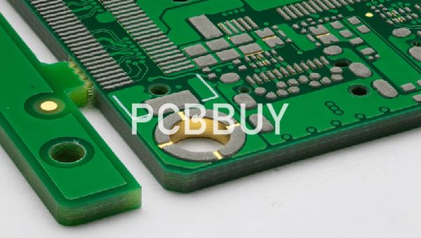
At PCBBUY, we source high-grade FR-4 base materials to ensure structural integrity and dielectric consistency. We offer a full range of material customizations including:
-
TG135-TG170 options for thermal reliability
-
Halogen-free materials for environmentally safe applications
-
CTI-rated substrates for high-voltage endurance
All materials are RoHS compliant, and special materials can be reviewed and customized according to your project specifications.
Flexible HDI PCB Stacking
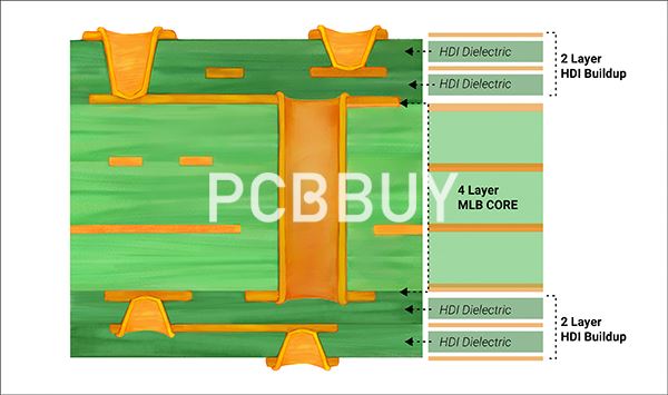
When it comes to HDI PCB stack-up, PCBBUY supports:
-
1st-order HDI: 4–10 layers
-
2nd-stage HDI: 6–10 layers with sequential lamination
Multilayer configurations are tailored for signal integrity and impedance control, making them ideal for mobile devices, wearable electronics, and high-frequency systems.
Construction Types Optimized Structures for Compact Design
Our engineering team provides precision construction types such as:
-
1st-order HDI examples: 1+N+1, 1+1+N+1+1
-
2nd-order HDI examples: 2+N+2, 1+2+N+2+1
All vias ≤ 0.3mm are supported. Depending on your stack-up and routing requirements, we use either internal mechanical vias or filled electroplated microvias.
Trace Width and Spacing
-
Minimum trace width/spacing: 2/2 mil (0.05/0.05mm)
This allows us to support high-speed and high-density applications without compromising signal integrity. Our photolithography process ensures edge definition with tight tolerance.
Blind Via Technology
PCBBUY offers both mechanical and laser drilling for blind vias:
-
Mechanical blind vias: ≥ 0.15mm diameter
-
Laser blind vias: ≥ 0.075mm diameter
Each type is reviewed per customer spec. Laser vias allow for higher density interconnection while mechanical vias offer robustness for inner-layer connectivity.
Hole Size
-
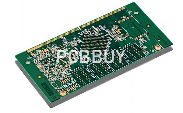
Minimum unilateral hole size: ≥3 mil (0.076mm)
Our laser and mechanical drills are calibrated regularly to ensure precision. We also support via-in-pad designs for BGA packages, helping to reduce component footprint.
Hole Copper Thickness
-
No laser blind burial: Mechanical hole copper >18μm
-
Laser blind burial: Mechanical hole copper >13μm
All plating thicknesses are verified using cross-section and X-ray analysis. Customized plating is available depending on current-carrying or thermal dissipation requirements.
Via Electroplating
-
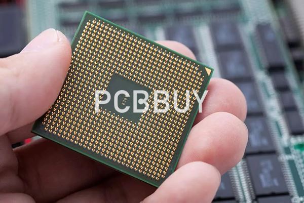
Via Electroplating Depth: 0.05mm to 0.1mm
-
Tolerance: ±15%
PCBBUY uses advanced copper electroplating techniques to ensure the entire hole wall is fully metalized. Our process fills the via from bottom to top to avoid voids and ensure maximum reliability under thermal cycling.
Why Choose PCBBUY for HDI PCB China Manufacturing
With years of experience and advanced HDI production lines, PCBBUY provides:
-
Quick turnaround prototyping to volume production
-
Dedicated engineering review for DFM and DFA
-
Full-stack customization: stack-up, copper weight, via type, surface finish
-
International shipping and multilingual customer service
We support end-markets from automotive and medical to aerospace and IoT. When searching for a reliable "HDI PCB China" partner, choose PCBBUY for proven capability and global trust.
Ready to Start Your Project?
Contact us now for a free design review or instant quotation. Upload your Gerber files or chat with one of our technical consultants. Let PCBBUY take your next-generation HDI PCB from design to delivery with precision and care.
Industry Category


