Hard Gold PCB Finish PCBBUY’s Advanced Manufacturing Process
By:PCBBUY 08/29/2025 16:40
Introduction to Hard Gold PCB Finish
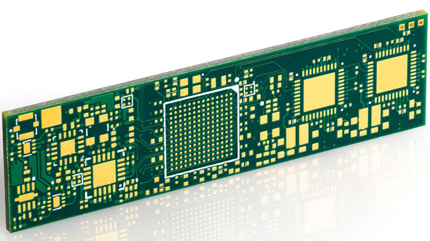
The hard gold PCB finish is one of the most durable and long lasting surface treatment in high-reliability electronics manufacturing. Hard gold finish (electroplated hard gold) is designed to survive heavy wear and frequent mechanical contact unlike immersion gold that provides the maximum flatness and solderability.
We are PCBBUY, and we are the company that focuses on the provision of hard gold PCB solutions with a tight control over the depth of gold, alloy mix, and plating uniformity that will ensure consistent performance in the harsh environments of connector usage, gold fingers, and military electronics.
What is Hard Gold PCB Finish?
Hard gold PCB finish Hard gold PCB finish is a nickel through barrier electroplated gold finish on a printed circuit board. This is done by means of electrochemical deposition and this enables it to customize both the nickel and gold thickness:
• Nickel layer thickness: 120–200μ''
• Gold layer thickness: 1–100μ''
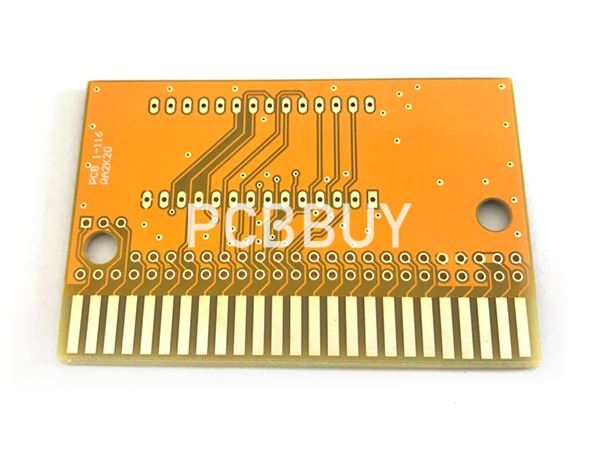
Materials like nickel, cobalt, palladium, chromium, or bismuth are alloyed with the gold layer, and increase hardness and wear resistance greatly over soft or immersion gold. At PCBBUY, these parameters can be adapted to the specifications of the customers, be it partial plating (like edge connectors) or full board hard gold plating.
Advantages of Hard Gold PCB Finish
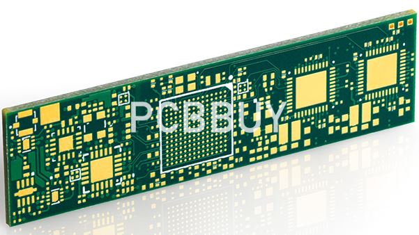
Hard gold PCB finish offers the following major advantages:
1. Superior Wear Resistance - Excellent in gold fingers and connector pads where the insertion and removal are frequent.
2. Extended Product Lifespan – Maintains stable conductivity even after thousands of mechanical cycles.
3. Excellent Electrical Performance – Provides low and stable contact resistance.
4. Corrosion and Oxidation Resistance – Ensures long-term reliability even in harsh environments.
5. Adaptable Thickness- At PCBBUY, customers have an option to order nickel and gold layers of various thicknesses, according to their use.
Hard gold is selected over immersion gold PCB finish (ENIG), where solderability and flatness take priority, whereas the durability and mechanical strength are the primary concerns.
PCBBUY’s Expertise in Hard Gold PCB Finish
Our hard gold plating methodology at PCBBUY aims at achieving accuracy, stability, and consistency of each order. We have technical capabilities such as:
Gold Thickness Control: Variable 1-100mu, with applications to both high-frequency connectors and heavy-industrial.
Nickel Barrier Layer Accuracy: Controlled in the range of 120-200mu inches to give excellent adhesion and prevent diffusion.
Alloy Customization: There is the choice of gold-nickel, gold-cobalt, gold-palladium, gold-chromium, and gold-bismuth alloys which are best suited in hardness and conductivity.
Advanced Electroplating Line: The automated plating equipment is designed so as to provide consistent coverage and reduce variance across the board.
Comprehensive Quality Inspection: Every PCB undergoes thickness measurement (XRF), hardness testing, contact resistance verification, and environmental reliability tests.
Hard Gold PCB Finish Manufacturing Process at PCBBUY
The manufacturing procedure of PCBBUY is based on the high-quality and precision standards:
1. Surface Preparation- Board cleaning and micro-etching to leave them with no contaminants.
2. Nickel Plating – Deposition of a 120–200μ'' nickel barrier layer for diffusion resistance.
3. Gold Electroplating – Controlled application of 1–100μ'' gold with specified alloy composition.
4. Thickness & Hardness Testing- X-ray fluorescence (XRF) and mechanical testing to confirm the thickness and hardness of the gold.
5. Final Quality Assurance – Electrical performance, adhesion, and wear-resistance tests before delivery.
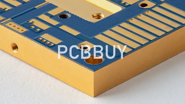
Applications of Hard Gold PCB Finish
Hard gold PCB finish is common in:
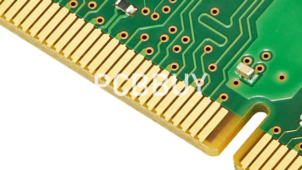
• Gold fingers and connectors (PCIe, memory modules, server boards)
• High-frequency & high-speed PCBs
• Aerospace and defense electronics
• Industrial control systems and automotive PCBs
Medical equipment that has long lifespan.
Why Choose PCBBUY for Hard Gold PCB Finish?
Precision and consistency are imperative when it comes to hard gold finishes and determining a PCB manufacturer. PCBBUY stands out with:
• Plating specification that is customizable based on various applications.
• Strict international certifications (ISO, UL, RoHS) for global compliance
• Well trained engineering workforce that guarantees design-for-manufacturing (DFM) support.
• Loose production capacity - prototype to mass production.
• International delivery system that guarantees rapid and dependable logistics services.
Conclusion
Hard gold PCB finish has been the best option where excellent durability, wear, and electrical reliability are required. Our advanced technology in plating, careful control of thickness, and thorough quality checking ensured HK-performance PCB solutions to our customers all over the world at PCBBUY.
PCBBUY provides high-quality and reliable performance whether you require gold fingers, connectors or the complete hard gold plating. Today, we invite you to contact our team and discuss the way in which we can make hard gold PCB finish make your electronic products more attractive.
Industry Category


