High Aspect Ratio Etching Explained Simply
By:PCBBUY 12/22/2025 16:48

High aspect ratio etching in PCB manufacturing refers to the process of etching fine copper traces where the ratio between copper thickness and line width is relatively high.
As PCB designs become denser and copper thickness increases, achieving clean and precise line profiles becomes significantly more challenging.
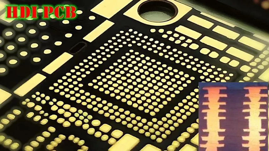
High aspect ratio etching is commonly required in advanced PCB fabrication, especially for HDI boards, fine-line multilayer PCBs, and high-reliability electronic products.
Why High Aspect Ratio Etching Is Technically Challenging?
Compared with standard PCB etching, high aspect ratio etching faces several critical challenges:
Increased risk of over-etching and under-etching
Difficulty maintaining uniform line width
Sidewall tapering and uneven copper removal
Reduced process window when copper thickness increases
These challenges require precise control of exposure, plating uniformity, etching chemistry, and equipment stability.
Typical PCB Products That Need High Aspect Ratio Etching
HDI and fine line PCBs
High-speed digital boards
Automotive and industrial PCBs
Compact multilayer designs
These products demand precise control throughout the etching process.

How PCBBUY Supports High Aspect Ratio Etching?
PCBBUY ensures stable high aspect ratio etching through:
Mature fine-line etching technology
Consistent copper plating control
Reliable exposure and etching equipment
Engineering support from design to production
Whether for prototypes or volume orders, PCBBUY maintains consistent etching quality.
Design Tips for Better Etching Results
To improve manufacturability, customers are encouraged to:
Balance line width and copper thickness
Avoid extreme designs without technical evaluation
Consult PCBBUY engineers during the design stage
Early communication helps reduce risk and improve yield.

Why Choose PCBBUY?
With strong technical expertise and experience serving overseas customers, PCBBUY is a reliable partner for high aspect ratio etching PCB fabrication.
FAQ
What is high aspect ratio etching in PCB?
High aspect ratio etching refers to the PCB etching process used to create fine copper traces with a high ratio between copper thickness and line width.
Why is high aspect ratio etching difficult?
It requires precise control of copper thickness, photoresist accuracy, and etching parameters to avoid over-etching, under-etching, and line deformation.
What PCB applications require high aspect ratio etching?
HDI PCBs, fine line multilayer boards, high-speed PCBs, and industrial or automotive electronics commonly require high aspect ratio etching.
Can PCBBUY support high aspect ratio etching designs?
Yes. PCBBUY supports high aspect ratio etching through optimized processes, advanced equipment, and engineering DFM review.
How can I improve my PCB design for high aspect ratio etching?
Balancing copper thickness and line width, allowing proper tolerances, and consulting with PCBBUY engineers during design can improve etching results.
Industry Category


