High Current PCB Design Guidelines: 5 Effective Tips to Manufacturing
By:PCBBUY 10/21/2021 08:59

Working with high power circuits does involve some different PCB design techniques, such as the width and weight of the copper that is used on the board. As fascinating and intricate as the process of designing and executing a printed circuit board or PCB design is. Although these tools are not standardized, they can be quite helpful in designing PCBs that are capable of meeting their current capacity requirements.
In this passage, we are going to provide you all the details about high current PCB. If you are going to learn knowledge of high current PCB, please check an read the content below for more information.
1. How to use shorter traces in high current PCB design?
When designing using high current applications, you need to know that shorter traces are more likely to work better. One thing is this, if the trace is longer, there are chances that you may experience bigger resistance. This implies that a longer trace may slow down your work. You do not want to experience any form of delay while working. This is why you have to be so cautious of the traces you use. You have to restrict the loss of any form of power. As a result of that, maintain the traces. Since you are into high current PCB design, it is paramount to go for the shorter traces.
2. How to remove solder mask in high current PCB design?
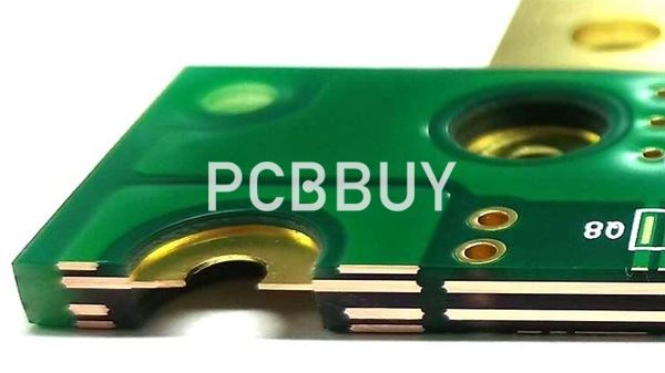
As a designer, one can remove the solder mask of the board. The high current PCB design requires that the board is always receiving connection. One method that guarantees that a trace transports a larger volume of current on the board is by eliminating one’s mask.
As a result, it reveals the basic copper matter. Some additional soldiers can help raise the thickness of your copper. This will then reduce the general resistance of the current transporting to the PCB. In the long run, your PCB can then adapt to some larger volume of current. It would not in any way raise the trace width.
3. What is the effect of high current PCB to design?
In 2009, the IPC-2152 Standard for Determining Current-carrying Capacity in Printed Board Design was released. This standard for relating trace width, copper weight and current carrying capacity replaced the long-standing and still often used the IPC-2221A standard. Based upon the guidelines of these standards, attempts to develop a reliable means of determining these parameters for high current PCBs have been made culminating in a number of on-line trace-width calculators, such as DigiKey, to assist developers and board designers. Although these tools are not standardized, they can be quite helpful in designing PCBs that are capable of meeting their current capacity requirements.
Most circuit boards process or transfer low power signals for digital, RF or power circuitry. For these applications, copper weights of 1oz or 2oz carrying currents in the mA to tens of amps range are typically sufficient. For some industries, such as military and aerospace, medical systems, automotive and industrial production, PCBs must have traces that are capable of carrying hundreds or thousands of amps. For these boards, trace widths must be much wider or copper weights must be higher.

4. What are the considerations of high current PCB?
Board layout should be considered from the very beginning of a design. The most important rule for high power circuit boards is to know your power path. The location and amount of power flowing through a circuit is a major factor when deciding the IC position and type and amount of heat dissipation required on the printed circuit board (PCB).
Many factors affect the amount of layout for a given design. These factors include:
· The amount of power flowing through the circuit
· The ambient temperature around the device and the board
· The amount of airflow around the device and the board
· The board material
· IC density on the board
5. How to guarantee the safety in high current PCB?
As with any circuit, the primary concern with a high current circuit is ensuring that it operates safely. There are a few potential issues that are unique with boards that drive such high powered loads. The main hazard is heat. No matter how well you design and lay out the board, more heat is produced than with a standard board. This must always be considered when the housing is made, and external vents/fans should be used. Something that I do on ALL designs that drive more than a few amps, is to have a dedicated temperature sensor on the PCB. This is a great firmware based failsafe. With the ability to monitor the temperature, you should always be able to react to any situation of overheating. To reduce the amount of heat produced on the board itself, it is best to choose components with low resistance.

The next potential safety hazard is regarding short circuits. Since the board is designed to drive high power devices, when shorted, it will be able to source a considerable amount of current. It is crucial to consider this possibility in the design phase. The easiest way to deal with shorts is to have a fuse on ALL outputs that leave the board, and an input fuse. The fuses should always be rated for less current than the wires used can handle. They also should be rated for less/equal the amount of current the board traces/pours are designed for. It is also a good idea to use drivers that have built-in short circuit prevention built into them.
Industry Category


