High Layer Count PCB Yield Improvement
By:PCBBUY 01/30/2026 17:13
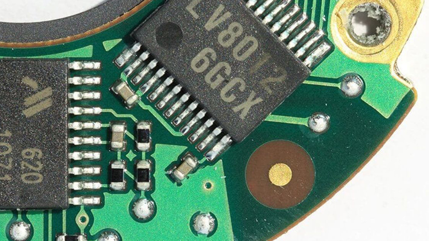
As electronic products continue to demand higher density and functionality, high layer count PCBs have become increasingly common in advanced applications. However, as layer count increases, manufacturing complexity rises significantly, making yield improvement a critical concern for PCB manufacturers and customers alike.
This article explores the key factors influencing high layer count PCB yield improvement and explains how professional manufacturing processes help achieve stable quality and cost-effective production.
What Is Considered a High Layer Count PCB?
In the PCB industry, boards with 16 layers or more are generally considered high layer count PCBs. For certain applications, layer counts may reach 24, 30, or even higher.
Typical applications include:
-
High-speed communication equipment
-
Industrial control systems
-
Medical electronics
-
Advanced computing hardware
As layer count increases, the number of process steps multiplies, and small variations can accumulate into significant yield loss.
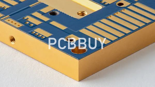
Key Factors Affecting Yield in High Layer Count PCB
Material Consistency
High layer count PCBs require large quantities of prepreg and core materials. Variations in resin content, thickness, or glass weave can lead to uneven lamination and internal defects, directly reducing yield.
Lamination Complexity
Multiple lamination cycles increase the risk of:
-
Resin starvation
-
Lamination voids
-
Delamination
Each additional press cycle introduces cumulative thermal and mechanical stress.
Drilling Accuracy and Aspect Ratio
High layer count boards typically involve:
-
Deeper drilling
-
Higher aspect ratio vias
-
Tighter positional tolerance
Any drilling deviation can cause via defects or layer misregistration.
Registration Control
Precise layer-to-layer alignment becomes more difficult as the number of layers increases. Poor registration directly impacts electrical connectivity and reliability.
Copper Balance and Stress Accumulation
Uneven copper distribution across layers can cause:
-
Warpage
-
Resin flow imbalance
-
Internal stress concentration
These issues often result in yield loss during lamination or thermal testing.
Design-Related Challenges That Reduce Yield
Design decisions have a major impact on manufacturing yield. Common design-related yield risks include:
-
Asymmetrical stackups
-
Extreme copper density variation
-
Overly complex via structures
-
Lack of early DFM coordination
Without manufacturing-oriented design optimization, even advanced factories struggle to maintain stable yield.
Process Strategies for High Layer Count PCB Yield Improvement
Stackup Engineering and Simulation
Professional manufacturers optimize stackups by:
-
Maintaining symmetry
-
Balancing dielectric thickness
-
Controlling copper distribution
Simulation and historical data help predict lamination behavior before production.
Advanced Lamination Control
Yield improvement depends heavily on lamination control, including:
-
Vacuum-assisted lamination
-
Optimized temperature ramp profiles
-
Controlled pressure distribution
-
Multi-stage curing processes
These methods reduce internal defects and improve interlayer bonding.
Precision Drilling and Via Formation
To maintain yield, manufacturers employ:
-
High-precision drilling equipment
-
Controlled drill wear monitoring
-
Optimized via plating processes
Consistent via quality is essential in high layer count boards.
Inline Inspection and Process Monitoring
Early defect detection is critical. Inline inspection methods help identify:
-
Registration drift
-
Thickness variation
-
Process instability
This allows corrective action before yield loss escalates.
Manufacturing Environment and Process Discipline
High layer count PCB production requires strict environmental control:
-
Low-humidity material storage
-
Controlled lamination room conditions
-
Standardized handling procedures
Process discipline ensures repeatability across long production cycles.
How PCBBUY Improves Yield for High Layer Count PCB?
PCBBUY focuses on systematic yield improvement through:
-
Carefully qualified material systems
-
Engineering-driven stackup optimization
-
Controlled lamination and drilling processes
-
Continuous in-process inspection
By integrating design review with manufacturing execution, PCBBUY helps customers achieve stable yield even in complex high layer count PCB projects.
Conclusion
High layer count PCB yield improvement is not achieved through a single process upgrade but through end-to-end manufacturing control. From material selection and stackup design to lamination, drilling, and inspection, every step influences final yield.
Working with an experienced PCB manufacturer that understands high layer count challenges is essential for achieving reliable quality and cost efficiency.
FAQ
What affects yield in high layer count PCB manufacturing?
Yield is affected by material consistency, lamination control, drilling accuracy, registration precision, and copper balance.
Why does PCB yield decrease as layer count increases?
Higher layer counts introduce more process steps, tighter tolerances, and accumulated thermal stress, increasing the risk of defects.
Can PCB design impact high layer count yield?
Yes. Stackup symmetry, copper balance, and via structure design have a direct influence on manufacturing yield.
How do manufacturers improve yield for high layer count PCBs?
Through optimized stackup engineering, advanced lamination techniques, precision drilling, and strict process control.
What layer count is considered high in PCB manufacturing?
Typically, PCBs with 16 layers or more are considered high layer count, though this may vary by application.
Industry Category


