High speed PCB design guidelines
By:PCBBUY 07/01/2021 17:35

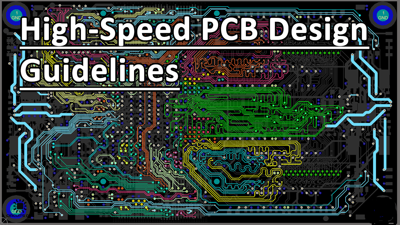
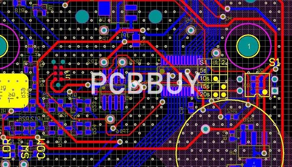
Whenever you have signals on a PCB that have high-speed edge rates, they then become dependent on minute factors in the PCB layout. These signals can lose integrity and are affected by physical parameters such as board stack-up, impedance, loop area, general design, and package type.
So a PCB design process that is optimized to retain signal integrity for these fast-changing signals is referred to as a high-speed PCB design. A high-speed design uses high-grade PCB materials with tight fiber interwinding and close tolerances and controlled impedance.
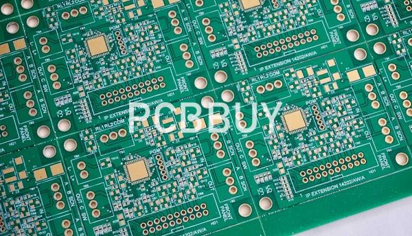
High-speed designs would also try to use small component packages such as BGA, LGA, MSOP, etc., instead of larger packets. Come and check the content we provide below for more tips about high speed PCB design.

What are the challenges of high speed PCB design?
The following section will highlight the main design challenges when it comes to designing high-speed PCBs
Tolerances
Since even minimal PCB characteristics can affect signal behavior, your manufacturer needs to have tight tolerances. These are tolerances typically for things like controlled impedance traces, board Stackup, and capacitance, and also the overall length and width of marks.
Availability of high-speed material
Beyond certain speeds, you may start to require the use of unique PCB material if the signals get too fast. Standard FR4 based fiberglass is not the best when it comes to designing high-speed boards. A few of the PCB materials used for high-speed designs are enhanced FR-4, Polyamide, PTFE.
Selecting the correct Layer Stackup
Another critical factor, especially in multi-layer boards, is selecting the right Layer Stackup, were to have a thick prepreg layer, where to have your power and ground planes, and also the separation between the sheets. All these factors, when chosen correctly, will improve signal integrity.
Board to Board Interconnections
When a design has multiple high-speed boards that need to be connected, it is essential to use a interconnect that can properly transmit high-speed signals, typically these will be shielded and length matched cables. The connectors would have their pins oriented in a way to minimize and signal losses.
What are the skills of high speed PCB design?
Knowing a design software that is capable of advanced options
High-speed designs require many sophisticated features in your CAD software. Many programs intended for hobbyists may not have these. Web-based suites also don't usually have advanced options. So one needs to learn and be skilled at a power CAD tool.
High-Speed Routing
A designer needs to know the rules for necessary routine when it comes to high-speed traces. It would include things such as not cutting ground planes and keeping trails short. Keeping digital lines not too close to avoid crosstalk, and shielding any interference producing elements so that signal integrity is not compromised.
Routing traces with controlled impedance
Certain types of signals require impedance matching. These are usually in the order of 40-120 ohms. Characteristic impedance matched hints are Antennae and many differential pairs.

The designer must be familiar with how to calculate trace width and layer stack for required impedance values. If a trace does not have the correct impedance value, the signal can be severely degraded, resulting in data corruption.
Length matching traces
High-speed memory busses and interface buses have many lines. These lines operate at very high frequency, and so the signals must arrive from the sending end to the receiving end at the same time. It requires a feature called length matching. Most common standards define tolerance values that must match length.
Minimizing loop area
High-speed PCB designers must know that high-frequency signals cause a lot of EMI, EMC issues. To minimize these issues, they must follow basic rules like having continuous ground planes and reducing loop areas by optimizing current return paths for traces and putting in lots of stitching vias.
What are the considerations of high speed PCB design?
The following are the most important design considerations when designing high-speed PCBs
Signal reflections
When signal is high-speed, the trace acts as a transmission line with characteristic impedance. To minimize and reflections along the trail, it is required to match the line impedance with the signal source impedance.
Signal ringing
Signal ringing is when you have some unwanted shifting in the voltage or current on the transmission line, which causes extra current to flow and causes delays in the arrival of your signal at its final destination. It can be an issue with messages such as a high-speed clock line. So these signals should be shielded from any interference.
Crosstalk issues
When two traces with high-speed signals are close together, then they can induce voltages into each other. So it is essential not to place such marks too close to prevent interference with each other.
Signal timing
If two traces carry high-speed signals and their lengths are different, then the messages arrive at their destination and slightly different times; this can be a big issue if the message is supposed to be synchronized to a standard clock line. In these cases, one needs to length match signals.
Industry Category


