
How Copper Distribution Improves PCB Manufacturing Quality and Long-Term Reliability?
By:PCBBUY 07/23/2026 14:40
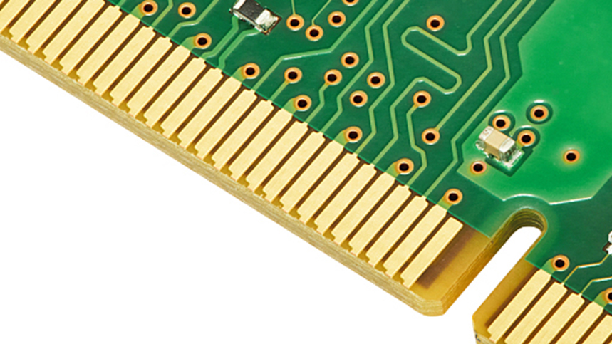
As PCB designs become increasingly complex, manufacturers are challenged not only by finer traces and higher layer counts but also by uneven copper distribution. Without proper copper balancing, printed circuit boards are more susceptible to warpage, lamination defects, etching inconsistencies, and dimensional instability, all of which can affect both manufacturing yield and long-term reliability.
Understanding PCB copper balancing techniques for reliable fabrication is essential for engineers designing multilayer, HDI, automotive, industrial, and high-power PCBs. This article explains why copper balancing matters, explores common balancing methods, and demonstrates how PCBBUY ensures consistent PCB quality through advanced engineering and manufacturing controls.
What Is PCB Copper Balancing?
Copper balancing is the practice of maintaining a relatively uniform copper distribution across all PCB layers. Instead of allowing large copper-free areas adjacent to heavy copper regions, engineers intentionally adjust copper patterns so that heat, pressure, and plating current remain evenly distributed throughout fabrication.
Proper copper balancing benefits multiple manufacturing processes, including:
-
Inner-layer imaging
-
Etching
-
Lamination
-
Electroplating
-
Surface finishing
-
Mechanical drilling
-
Reflow assembly
The goal is to create a mechanically stable PCB that maintains consistent electrical and dimensional performance.
Why Copper Balance Is Important?
Copper imbalance creates differences in thermal expansion and mechanical stress during manufacturing.
Common consequences include:
-
PCB warpage
-
Resin flow imbalance
-
Lamination voids
-
Copper thickness variation
-
Poor impedance consistency
-
Registration errors
-
Reduced solder joint reliability
For high-layer-count or high-speed PCBs, these issues can significantly reduce manufacturing yield and field reliability.
Common PCB Copper Balancing Techniques
|
Technique |
Purpose |
Manufacturing Benefit |
|
Copper Thieving |
Add isolated copper in sparse areas |
Improves plating uniformity |
|
Copper Pour Optimization |
Balance copper density |
Reduces thermal stress |
|
Dummy Copper Patterns |
Equalize copper distribution |
Improves etching consistency |
|
Cross-Hatched Copper |
Maintain electrical performance while reducing copper mass |
Better dimensional stability |
|
Symmetrical Layer Design |
Balance top and bottom copper |
Reduces PCB warpage |
|
Balanced Plane Design |
Uniform power and ground planes |
Improves lamination quality |
Each technique serves a different purpose, and multiple methods are often combined within a single PCB design.
How Copper Balancing Improves Reliable Fabrication?
1. Reduces PCB Warpage
Uneven copper causes one side of the board to expand differently during lamination and soldering.
Balanced copper distribution helps:
-
Minimize board twisting
-
Reduce bow and twist
-
Improve SMT assembly accuracy
This is especially important for BGAs and fine-pitch components.
2. Improves Lamination Quality
During multilayer lamination, resin flows differently depending on copper density.
Balanced copper helps achieve:
-
Uniform resin flow
-
Better dielectric consistency
-
Lower risk of voids and delamination
This becomes increasingly important for high-layer-count PCBs.
3. Enhances Electroplating Uniformity
Copper plating current naturally concentrates in dense copper regions.
Balanced panel design helps maintain:
-
Uniform plated copper thickness
-
Stable via reliability
-
Consistent hole copper quality
This directly improves long-term electrical reliability.
4. Supports Controlled Impedance
Copper density affects dielectric thickness after lamination.
Improved copper balance contributes to:
-
Stable dielectric spacing
-
More accurate impedance values
-
Better signal integrity for high-speed applications
5. Improves Thermal Stability
Copper acts as a heat conductor.
Balanced layouts distribute thermal energy more evenly during:
-
Reflow soldering
-
Thermal cycling
-
High-power operation
This reduces localized thermal stress and extends PCB service life.
Copper Density Recommendations
|
PCB Type |
Recommended Copper Distribution |
|
Standard Multilayer PCB |
Relatively uniform across layers |
|
HDI PCB |
Carefully balanced around microvias |
|
High-Speed PCB |
Balanced near impedance-controlled traces |
|
Thick Copper PCB |
Extra balancing required to manage thermal expansion |
|
Automotive PCB |
Tight copper symmetry for reliability |
|
High-Power PCB |
Balanced copper planes for heat dissipation |
Engineering review is essential to determine the appropriate balancing strategy for each design.
PCBBUY's Copper Balancing Capabilities
PCBBUY incorporates copper balancing analysis into both DFM review and manufacturing engineering, helping customers achieve higher fabrication yields and more reliable PCB performance.
|
Manufacturing Capability |
PCBBUY Capability |
|
PCB Layers |
1–26 Layers |
|
Minimum Line/Space |
35 μm (1.4 mil) |
|
Minimum Mechanical Hole |
0.10 mm |
|
Thick Copper Capability |
Up to 15 oz |
|
Controlled Impedance |
Single-ended & Differential |
|
HDI Technology |
1st–3rd Order HDI |
|
Material Options |
FR-4, High-Tg, Rogers, TUC, Isola, Halogen-Free |
|
Engineering Review |
Copper balancing & DFM optimization |
|
Quality Inspection |
AOI, Flying Probe Test, X-ray Inspection, Cross-Section Analysis |
By combining engineering analysis, process optimization, and strict quality control, PCBBUY helps minimize manufacturing risks caused by uneven copper distribution.
Design Best Practices for Copper Balancing
To improve fabrication reliability, PCB designers should:
-
Maintain similar copper density across adjacent layers.
-
Use dummy copper or copper thieving where necessary.
-
Keep power and ground planes as symmetrical as possible.
-
Review copper distribution before finalizing the stack-up.
-
Consider thermal expansion when designing thick copper or high-current PCBs.
-
Work closely with the PCB manufacturer during the DFM stage.
Early collaboration between designers and manufacturers can significantly reduce production risks and improve first-pass yield.

FAQ
Q1: What is copper balancing in PCB fabrication?
Copper balancing is the process of creating a more uniform copper distribution across PCB layers to improve fabrication consistency, reduce stress, and enhance overall board reliability.
Q2: Why is copper balancing important for multilayer PCBs?
Multilayer PCBs experience greater thermal and mechanical stress during lamination. Balanced copper distribution helps prevent warpage, improves resin flow, and maintains layer registration accuracy.
Q3: Does copper balancing affect signal integrity?
Yes. Stable copper distribution helps maintain consistent dielectric thickness and controlled impedance, which are essential for high-speed signal transmission.
Q4: Is copper thieving the same as copper balancing?
No. Copper thieving is one technique used to improve plating uniformity, while copper balancing refers to the broader strategy of optimizing copper distribution throughout the PCB design.
Q5: Can PCBBUY review copper balance before production?
Yes. PCBBUY's engineering team performs comprehensive Design for Manufacturability (DFM) reviews, including copper distribution analysis, stack-up evaluation, impedance verification, and manufacturing optimization recommendations before production begins.
Conclusion
Proper PCB copper balancing techniques for reliable fabrication are essential for producing high-quality, high-reliability circuit boards. Balanced copper distribution improves plating uniformity, reduces warpage, enhances impedance stability, and increases long-term mechanical and electrical reliability.
With expertise in multilayer PCB fabrication, HDI technology, thick copper manufacturing, controlled impedance processing, and advanced DFM engineering, PCBBUY delivers manufacturing solutions that help customers transform complex PCB designs into reliable, production-ready products for industries including industrial automation, automotive electronics, telecommunications, aerospace, medical devices, and AI computing.
Industry Category








