
How Does PCB Copper Roughness Affect Signal Integrity?
By:PCBBUY 08/25/2026 16:17
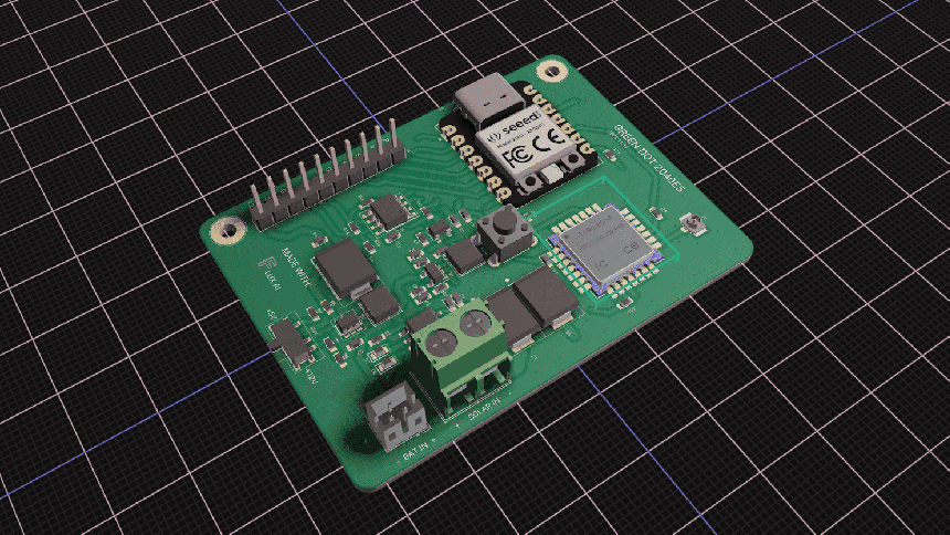
When engineers investigate signal integrity problems in a high-speed PCB, they often focus first on dielectric loss, impedance mismatch, crosstalk, vias, or stackup design. Copper surface roughness is sometimes overlooked. That can be a mistake.
As signal frequency increases, current does not distribute uniformly throughout the entire copper conductor. Instead, the current becomes increasingly concentrated near the conductor surface due to the skin effect. If that surface is significantly rough, the actual path followed by the high-frequency current becomes longer and more electrically complex than an ideal smooth conductor.
Copper roughness is an engineering trade-off involving signal frequency, copper type, conductor geometry, material selection, adhesion requirements, manufacturing process, and cost.
For automotive electronics, industrial control systems, energy-storage equipment, power electronics, new-energy systems, and embodied robotics, the correct question is therefore not simply:
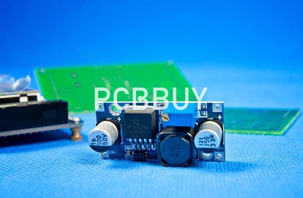
What Is PCB Copper Roughness?
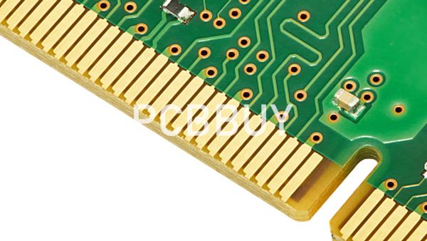
PCB copper roughness refers to the microscopic unevenness of a copper surface.
Copper foil is not perfectly flat. Its surface contains microscopic peaks, valleys, and irregularities.
The roughness depends on factors such as:
Copper foil manufacturing method
Copper treatment
Bonding treatment
Electroplating
Etching
Surface processing
Final copper thickness
In PCB manufacturing, copper surface characteristics are important because the copper must simultaneously provide:
Good electrical conductivity
Adequate mechanical adhesion
Reliable lamination
Sufficient resistance to thermal and mechanical stress
For conventional low-frequency circuits, the electrical impact of surface roughness may be relatively small.
For high-speed and high-frequency circuits, however, the situation becomes more complicated.
How Does Copper Roughness Increase Signal Loss?
Consider two copper surfaces.
Smooth copper
The high-frequency current travels along a relatively smooth conductive boundary.
Rough copper
The current encounters microscopic surface peaks and valleys.
The effective electrical path can become longer, increasing the effective resistance experienced by the high-frequency signal.
The simplified relationship can be expressed conceptually as:
Higher frequency → stronger skin effect → greater sensitivity to copper surface → potentially higher conductor loss
This is why copper roughness becomes increasingly relevant when PCB designs move from relatively low-speed digital signaling toward high-speed serial links, RF, microwave, and millimeter-wave applications.
Does Copper Roughness Affect Signal Integrity or Only Insertion Loss?
Copper roughness primarily becomes important through conductor loss, but signal integrity is a system-level result.
In a real high-speed PCB, signal quality depends on multiple loss mechanisms:
Conductor loss
Dielectric loss
Reflection loss
Via discontinuities
Impedance mismatch
Crosstalk
Connector transitions
Return-path discontinuities
Copper roughness therefore should not be treated as an isolated signal-integrity problem.
For example, if a transmission channel already has significant dielectric loss and impedance discontinuities, reducing copper roughness alone may not solve the overall signal-integrity problem.
On the other hand, when a high-speed channel has a tight insertion-loss budget, conductor loss can become significant enough that copper surface characteristics deserve explicit consideration.
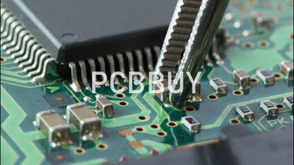
What Happens to a High-Speed PCB When Copper Roughness Is Too High?
Excessive conductor loss can contribute to several electrical problems.
1. Higher Insertion Loss
More energy is dissipated as the signal travels along the trace.
This reduces the signal amplitude arriving at the receiver.
2. Reduced High-Frequency Bandwidth
Loss is generally frequency-dependent.
As frequency increases, the influence of conductor surface characteristics can become more pronounced.
3. Greater Eye-Pattern Degradation
For high-speed digital interfaces, additional channel loss can reduce eye height and eye width.
4. Increased Inter-Symbol Interference
A frequency-dependent channel loss changes the shape of the received waveform.
This can contribute to inter-symbol interference and make receiver equalization more difficult.
5. Reduced Channel Margin
In automotive, industrial, and robotics applications, a reduction in signal margin can become particularly important because the PCB may operate alongside switching power circuits, motors, sensors, and other sources of electromagnetic noise.
How Does Copper Roughness Interact With PCB Trace Geometry?
The impact of copper roughness also depends on the transmission-line geometry.
Common high-speed structures include:
Microstrip
Stripline
Coplanar waveguide
Differential pairs
The electric and magnetic fields interact differently with the conductor surfaces in each structure.
For example, a stripline is surrounded by dielectric material and reference planes, while a microstrip has a conductor exposed to the dielectric on one side and air on the other.
Therefore, copper roughness should be considered together with:
Trace width
Trace spacing
Dielectric thickness
Copper thickness
Reference-plane distance
Differential-pair geometry
Operating frequency
This is why a PCB manufacturer's ability to control physical geometry matters just as much as the material selection itself.
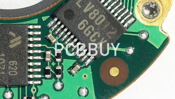
Why Does Copper Roughness Matter More as Frequency Increases?
At lower frequencies, the current penetrates deeper into the conductor.
The entire copper cross-section can contribute more effectively to conduction.
As frequency increases, skin depth decreases. The signal increasingly relies on the conductor surface.
Therefore, microscopic surface characteristics become more electrically significant.
This creates a general engineering trend:
PCB Operating Condition | Sensitivity to Copper Roughness | Main Concern |
Low-frequency power/control | Relatively low | DC resistance and current capacity |
Moderate-speed digital | Application-dependent | Overall channel loss |
High-speed serial | Increasing | Insertion loss and eye margin |
RF / microwave | High | Conductor loss and phase behavior |
Millimeter-wave | Very high sensitivity | Surface-dependent conductor loss and transmission-line performance |
The exact transition point depends on the complete channel, not on one universal frequency threshold.
How Does Copper Roughness Affect Differential Pairs?
Differential signaling is widely used in high-speed automotive, industrial, networking, computing, and robotics electronics.
A differential pair depends on the two conductors maintaining sufficiently similar electrical characteristics.
If the physical structure of the two traces differs significantly, their propagation and attenuation characteristics can become unbalanced.
Copper roughness is therefore one of several manufacturing variables that can influence high-speed differential channels.
However, it is important not to overstate the effect. In most practical differential-pair designs, engineers should evaluate copper roughness together with:
Trace width
Trace spacing
Copper thickness
Dielectric thickness
Layer-to-layer registration
Via symmetry
Reference-plane continuity
Connector transitions
In other words, copper roughness is part of the channel-loss budget rather than the entire differential-pair design problem.
How Does Copper Roughness Interact With Impedance Control?
Copper roughness does not simply mean that the nominal impedance changes by a fixed amount.Controlled impedance is primarily determined by the transmission-line geometry and dielectric environment.
However, manufacturing variations in:
Trace width
Copper thickness
Dielectric thickness
Layer registration
can affect actual impedance.
For this reason, a high-speed PCB manufacturer needs to control the physical geometry of the transmission line, not just specify a target impedance.
PCBBUY's current published process capability lists a general minimum impedance tolerance of ±10%. For example, a 50 Ω nominal design corresponds to a stated allowable range of 45–55 Ω under that tolerance. Tighter impedance requirements should be explicitly specified and technically reviewed for the particular project.
How Does PCB Etching Affect High-Speed Signal Integrity?
Copper roughness is only one part of the conductor-manufacturing process.
Etching also changes the final trace geometry.
During PCB fabrication, the designed trace width is translated into an actual copper pattern.
If the etching process changes the line width significantly, the resulting transmission-line impedance may differ from the design target.
The current PCBBUY process specification lists a standard ±20% line-etching tolerance, with 10% available by specification. The same document gives a ±2 mil capability for external-layer image-to-hole positioning.
This is particularly relevant for high-speed PCB design. For example, if a high-speed transmission line is designed with a narrow trace, the engineering team should evaluate whether the required trace width, copper thickness, and etching tolerance are compatible with the desired impedance.
This is a better approach than designing first and asking the PCB manufacturer to "make it work" later.
How Does Copper Thickness Affect Signal Integrity?
Copper thickness affects both electrical and manufacturing behavior.
PCBBUY's current process capability specifies:
Outer-layer finished copper: 1–4 oz as the conventional range
Customized outer-layer copper up to 15 oz
Inner-layer finished copper: H oz–3 oz as the conventional range
Customized inner-layer copper up to 8 oz
However, these are manufacturing capability ranges, not recommendations that high-speed signal layers should use maximum copper thickness.
For a high-speed channel, copper thickness should be selected based on:
Target impedance
Trace width
Signal frequency
Conductor loss
Current requirements
Manufacturing capability
For example, a power layer may require substantially more copper than a high-speed signal layer.
Therefore, mixed copper thickness across different layers can be appropriate when the stackup and manufacturing process support it.
Why Is Copper Roughness Especially Important for Automotive PCB Applications?
Automotive electronics increasingly combine high-speed communication with sensing, control, power conversion, and computing.
Typical systems may include:
Automotive radar
Cameras
Sensor modules
ADAS electronics
Vehicle communication
Motor control
Battery management
Power conversion
These systems often require reliable signal transmission under changing temperature and mechanical conditions.
For automotive high-speed PCB designs, copper roughness should therefore be evaluated as part of a larger reliability and signal-integrity strategy.
The goal is not to select the smoothest possible copper in isolation.
The goal is to establish a repeatable copper/dielectric/trace system that meets the required electrical performance throughout production.

Why Does Copper Roughness Matter for Industrial Control and Robotics?
ndustrial control and embodied robotics often combine high-speed digital interfaces with motors and power electronics.
A robotic controller may contain:
High-speed processors
Ethernet interfaces
Sensor interfaces
Motor-control circuits
Power converters
RF or wireless modules
These functions create different PCB requirements.
A high-current layer may need relatively thick copper, while a high-speed communication layer may prioritize controlled transmission-line geometry and low loss.
This is where stackup engineering becomes important.
The PCB manufacturer should understand which layers are:
high-current → high-speed → RF → ground → power
rather than treating all copper layers as electrically equivalent.
How Should Copper Roughness Be Specified for a High-Speed PCB?
A common mistake is to specify only:
"Use low-roughness copper."
That is not sufficiently precise.
A better engineering specification should identify the electrical requirement first.
For example:
Operating frequency
Data rate
Channel length
Target insertion loss
Differential impedance
Maximum acceptable loss
Material type
Copper thickness
Copper surface requirement, if applicable
Stackup
Testing requirements
If copper roughness is critical to the channel budget, the required copper foil type or surface specification should be explicitly discussed with the PCB manufacturer.
This prevents the manufacturer from having to infer an unstated RF requirement.
What Copper Parameters Should Be Reviewed Before Production?
For high-speed PCBs, I recommend reviewing the following parameters together:
Parameter | Why It Matters to Signal Integrity | What Should Be Controlled? |
Copper roughness | Influences high-frequency conductor loss | Appropriate copper surface/foil specification |
Copper thickness | Changes conductor geometry and loss | Layer-specific finished copper |
Trace width | Affects impedance and loss | Fabrication-compatible line width |
Trace spacing | Affects coupling and crosstalk | Defined by SI analysis |
Dielectric thickness | Changes impedance and field distribution | Controlled stackup |
Dk / Df | Determines dielectric behavior and loss | Material-specific data |
Etching accuracy | Changes actual trace geometry | Defined etching tolerance |
Layer registration | Affects alignment between signal and reference structures | Controlled registration |
Via geometry | Creates discontinuities and parasitic effects | Via size, pad, anti-pad and stub control |
Impedance | Directly affects reflections | Design target and test requirement |
The important point is that copper roughness should never be analyzed independently from the rest of the signal path.
How Can PCB Manufacturers Reduce the Impact of Copper Roughness?
A manufacturer can approach the problem from several directions.
1. Select the Appropriate Copper Foil
If the design has a strict high-frequency loss budget, the copper foil/surface specification should be reviewed during material selection.
2. Match Copper and Laminate
Copper treatment must provide adequate adhesion to the selected dielectric material.
The lowest-roughness option is not necessarily appropriate for every laminate system.
3. Control Finished Copper Thickness
The final conductor geometry should be consistent with the stackup and impedance design.
4. Control Etching
Trace geometry should remain within the specified manufacturing window.
5. Control Layer Registration
Signal layers must remain properly aligned with their reference planes and adjacent structures.
6. Verify the Finished PCB
Where applicable, impedance testing, electrical testing, coupons, and production inspection should be incorporated into the quality plan.
How Does PCBBUY's PCB Process Capability Support High-Speed Designs?
PCBBUY's published process capability provides several manufacturing controls that are relevant to high-speed and high-density PCB designs.
The manufacturing platform supports 1–26 layer PCBs and identifies Rogers and Taier high-frequency materials among its material options. It also supports conventional multilayer structures from 4 through 12 layers, with 14–26-layer structures reviewed according to customer process requirements.
For conductor geometry, the published capability includes fine-line processing and specifies different line/space ranges according to finished copper thickness. The document lists, for example, 3/3 mil design line/space for 1 oz copper, 6/6 mil for 2 oz, 10/10 mil for 3 oz, and 12/12 mil for 4 oz, with tighter limits identified separately.
This is important because copper thickness and trace geometry cannot be specified independently.
If a customer needs a high-speed trace with a particular impedance, the design should be checked against the actual copper thickness and etching process.
Can HDI Help With High-Speed PCB Signal Integrity?
HDI does not automatically improve signal integrity, but it can provide useful architectural advantages.
PCBBUY's documented HDI capability includes:
1st-order HDI: 4–16 layers
2nd-order HDI: 6–10 layers
Minimum HDI line/space: 2/2 mil
Mechanical blind via ≥0.15 mm
Laser blind via ≥0.075 mm
Minimum HDI hole diameter: 0.10 mm
Minimum single-side annular ring: 3 mil
For high-speed designs, HDI can be useful when the architecture requires:
Shorter interconnects
Higher routing density
Compact via transitions
Better layer allocation
Smaller component escape areas
The actual benefit depends on the signal-integrity architecture.
Why Is Layer Registration Important for High-Speed Signals?
A high-speed trace is not an isolated copper line.
It interacts electromagnetically with its reference plane.
If the relationship between the signal trace and its reference plane changes, the transmission-line characteristics can change.
Layer registration therefore becomes particularly important in:
Multilayer high-speed boards
Differential pairs
Controlled-impedance structures
HDI boards
RF sections
PCBBUY's published capability specifies an external-layer image-to-hole positioning accuracy of ±2 mil and layer-related positioning controls in its conventional PCB process.
For a demanding high-speed design, however, the appropriate tolerance should still be determined by the stackup and electrical requirements.

Summary
The PCB copper roughness effect on signal integrity becomes increasingly important as signal frequency rises.
Because high-frequency current concentrates near the conductor surface, copper surface characteristics can contribute to conductor loss. Excessive roughness can therefore increase insertion loss and reduce the available signal-integrity margin in demanding high-speed channels.
However, copper roughness should never be considered in isolation.
The actual performance of a high-speed PCB depends on the combined effect of:
copper roughness + copper thickness + trace geometry + dielectric properties + stackup + vias + impedance + manufacturing tolerances
For PCBBUY's PCB manufacturing process, the documented capabilities provide several relevant production foundations, including Rogers and Taier high-frequency materials, 1–26 layer production, controlled impedance, fine-line processing, HDI, customized copper thickness, and production testing options.
The published process data also specifies 1–4 oz conventional outer-layer finished copper, H oz–3 oz conventional inner-layer finished copper, ±20% standard line-etching tolerance with 10% available by specification, and ±2 mil external image-to-hole positioning capability.
For high-speed automotive electronics, industrial control boards, power and energy-storage systems, new-energy equipment, and embodied robotics, the best strategy is therefore not simply to request "smooth copper."
Instead, define the electrical loss budget first, then select the copper, laminate, stackup and manufacturing tolerances that can realistically deliver that requirement in production.
FAQ: PCB Copper Roughness and Signal Integrity
What is PCB copper roughness?
PCB copper roughness refers to the microscopic peaks and valleys on the surface of copper foil or copper conductors. It is a normal characteristic of copper manufacturing, but its electrical significance increases as signal frequency increases.
How does copper roughness affect signal integrity?
Copper roughness can increase high-frequency conductor loss because the signal current becomes concentrated near the conductor surface due to the skin effect. Higher conductor loss can contribute to increased insertion loss and reduced high-speed signal margin.
Does copper roughness affect impedance?
Copper roughness is not normally treated as a simple fixed impedance error. Impedance is strongly influenced by trace geometry and dielectric structure. Copper roughness mainly affects high-frequency conductor loss, although its electromagnetic effect can also influence the detailed behavior of a transmission line.
Is smoother copper always better?
No. Smoother copper can reduce high-frequency conductor loss, but the copper surface must also provide adequate adhesion and manufacturing reliability. The appropriate copper construction is a trade-off between electrical performance, reliability and manufacturability.
Does copper roughness matter for ordinary FR-4 PCBs?
It depends on the signal frequency and channel requirements. For conventional low-speed circuits, copper roughness may have relatively little impact on system performance. For high-speed serial, RF, microwave and millimeter-wave designs, it can become much more important.
Does copper thickness affect copper roughness?
Copper thickness and copper roughness are separate parameters. Thickness describes the physical conductor thickness, while roughness describes its surface profile. Both should be considered in high-frequency PCB design.
What other factors are more important than copper roughness?
There is no universal ranking. Depending on the application, dielectric loss, impedance discontinuities, via transitions, crosstalk, return-path problems, trace geometry and channel length can have equal or greater influence on signal integrity.
Can standard PCB copper be used for high-speed designs?
It can be, depending on the frequency and signal-loss budget. If the design has a tight insertion-loss requirement, the copper foil/surface specification should be reviewed as part of the complete channel design.
Does PCBBUY support high-frequency PCB materials?
Yes. The supplied manufacturing capability lists Rogers and Taier high-frequency materials, including Rogers 3000–4000 series documentation. The exact material grade should be selected according to the customer's design requirements.
What copper thickness can PCBBUY manufacture?
The published process capability lists 1–4 oz conventional finished copper on outer layers and H oz–3 oz on inner layers, with customized outer copper up to 15 oz and inner copper up to 8 oz.
What is PCBBUY's line-etching tolerance?
The published process capability lists ±20% line-etching tolerance, with 10% available by specification. High-speed designs with tight geometry requirements should be reviewed against the actual stackup and manufacturing process.
Can PCBBUY manufacture HDI high-speed PCBs?
Yes. The documented HDI capability includes 2/2 mil minimum line/space, 0.10 mm minimum HDI hole diameter and laser blind vias down to 0.075 mm, subject to engineering review for specific designs.
Can PCBBUY manufacture controlled-impedance PCBs?
Yes. The published general process capability specifies a minimum impedance tolerance of ±10%. If a project requires tighter impedance control, the requirement should be specified and evaluated during engineering review.
Can impedance testing be included before shipment?
The supplied process documentation identifies impedance reports and impedance coupons as applicable quality items and also lists flying-probe testing and other electrical inspection options. The exact outgoing test plan depends on the product specification.
What should I provide when ordering a high-speed PCB?
At minimum, provide the operating frequency/data rate, target impedance, stackup, material grade, copper thickness, trace geometry and relevant signal-integrity requirements. If copper roughness is critical to the loss budget, the required copper foil/surface specification should also be clearly stated.
Industry Category








