How Does PCB First Article Inspection Ensure Quality in Manufacturing?
By:PCBBUY 11/28/2024 16:33

Printed Circuit Board (PCB) manufacturing is a precise and intricate process critical to the production of electronic devices. To maintain quality and reliability, First Article Inspection (FAI) is a vital step in PCB production. FAI validates that the initial PCB produced meets all specified design requirements before full-scale production begins. This comprehensive inspection ensures the functionality, reliability, and manufacturability of the PCB, saving time and costs in the long run.
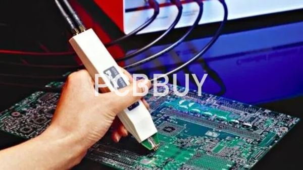
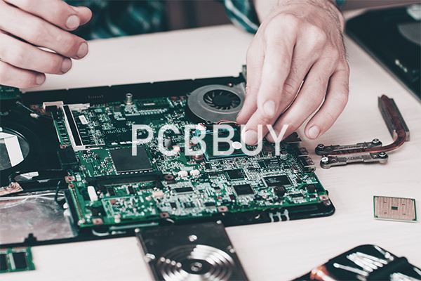
Inspecting your PCBs can uncover any defects that may have occurred during manufacturing or assembly. It can also help to reveal any design flaws that may exist. Checking PCBs after each phase of the process enables you to catch flaws before moving on to the next stage, which can save you from wasting further time and money on a defective product. It can also help you catch one-off defects that affect one or several PCBs. This process helps to ensure consistent quality among your boards and final products.

What Is PCB First Article Inspection?
Definition and Purpose
PCB First Article Inspection is the process of verifying the initial output from a manufacturing batch against the original design specifications, including mechanical, electrical, and aesthetic parameters. It acts as a quality gate, identifying discrepancies early in the manufacturing process.
Key goals of FAI:
-
Design Conformance: Ensure the PCB matches the customer's schematic and physical design.
-
Process Validation: Confirm the manufacturing process can consistently produce quality PCBs.
-
Risk Mitigation: Reduce defects in mass production by identifying and rectifying issues early.

Why we need PCB first article inspection?
Basically, the qualification report qualifies the processes used by the manufacturer, and the first article inspection verifies that these processes output a PCB as expected during normal production builds. First article inspection does not apply to procured vendor parts. Typically, it is used when the manufacturer builds to the customer’s technical data package, and the supplier has never previously built the PCB.
The first article inspection is a standard process to ensure the design characteristics of a PCB forwarded to the manufacturer actually meet design intent when the PCB is actually produced. The customer may repeat the first article inspection entirely or in part if there are changes such as:
· Change in the source or location where the PCB is produced
· If the design change significantly affects the form, fit, or functioning of the PCB
· If there is a significant change in the processes related to manufacturing, assembly, inspection, or testing
· If any manufacturing equipment has undergone a significant change
· If a natural or man-made occurrence adversely affects the manufacturing processes
· The production process has been interrupted for a significant amount of time
· There is significant degradation is test yields
· Any change in manufacturing and/or test personnel on the product line
· Any change in a vendor supplied item with an age factor or revision factor
Therefore, it is necessary for our customers to clarify the purpose of the first article inspection so that Rush PCB is able to mitigate the issues described above. Therefore, Rush PCB never treats first article inspection as just another check in the box, as many other suppliers do.

What Are Key Components of FAI?
1. Documentation Review
-
Cross-check the Gerber files, BOM (Bill of Materials), and assembly drawings.
-
Validate material specifications, stack-ups, and tolerances against customer requirements.
2. Physical Inspection
-
Inspect layer alignment, copper trace dimensions, via integrity, and solder mask quality.
-
Verify dimensions such as board thckness, hole sizes, and pad spacing using precise instruments like calipers and microscopes.
3. Electrical Testing
-
Conduct continuity and insulation tests to ensure correct electrical performance.
-
Validate impedance control for high-frequency circuits using time-domain reflectometry (TDR).
4. Functional Testing
-
Test for heat dissipation, power delivery, and signal integrity under simulated operational conditions.
Chemistry and Materials in PCB FAI
The inspection process often involves analyzing the materials used in PCB construction. These include:
Substrate Analysis
-
FR4 (Epoxy Fiberglass): Commonly used, inspected for dielectric properties.
-
Polyimide: Used in high-temperature applications, tested for thermal stability.
Example Reaction for Flame Retardants:
C6H3(PO3H2)2+H2O→C6H3(PO3)2+2H2O
Surface Finish
-
HASL (Hot Air Solder Leveling): Ensures uniform solderability; inspected for smoothness and thickness.
-
ENIG (Electroless Nickel Immersion Gold): Inspected for thickness and surface oxidation.
|
Finish Type |
Typical Thickness (µm) |
Inspection Method |
|
HASL |
1-25 |
Visual and contact gauge |
|
ENIG |
Gold: 0.05-0.1, Ni: 3-6 |
X-ray fluorescence (XRF) |
How to Prepare for PCB First Article Inspection?
Inspecting the first article units during the early stage ensures that engineers or technicians have the requisite understanding and consideration of the customer’s requirements and incorporated them into their manufacturing processes.

The pressure of reaching the market early tends to compress design schedules. This rushes the process of designing a new PCB assembly, testing it, and getting it ready for production, which often leads to errors. Customers, therefore, approach contract manufacturers like Rush PCB, due to their understanding and appreciation of an approval process such as the first article. A first article inspection process helps to identify potential issues in the early stages, so that the customer can take corrective actions.
Who conducts first article inspection?
FAI is extremely important for the yield of high-volume PCB assembly manufacturing, but who will play the role of conducting the first article inspection? In Technology, there are 3 options. First preferred is conducted by you, the customer, in our SMT assembly facility in Shenzhen. Because we can start mass production run in a very short time to get approved in our time if no defects found in the first articles. Then improve our work efficiency under the situation of no stop production. Second preferred is conducted by both sides of you and us online.
We show you the HD photos and transfer the inspection and testing results as per inspection and testing procedures and QC standards. This process always takes a little longer time than the first, and requires a longer time of stop PCB assembly production, but the inspection and testing will be more carefully and considerably by both sides. Third preferred is conducted by ourselves according to the inspection and testing procedures in both sides. The disadvantage of the third option is that the PCB assembly manufacturer may ignore something inspection or testing if you forget to specified.

What Is Process of Conducting PCB First Article Inspection?
Step 1: Preparing Inspection Criteria
-
Define criteria based on IPC standards (e.g., IPC-A-600 for acceptability).
-
Identify key design features to inspect, including traces, vias, and solder masks.
Step 2: Sample Preparation
-
Select the first manufactured PCB from the production line.
-
Clean and prepare the sample for inspection, ensuring no contamination affects results.
Step 3: Measurement and Testing
-
Optical Inspection: Use automated optical inspection (AOI) machines for defect detection.
-
Dimensional Analysis: Validate dimensions using coordinate measuring machines (CMM).
-
Electrical Testing: Perform flying probe or in-circuit testing for short circuits and open circuits.
Step 4: Documentation and Reporting
-
Compile an FAI report summarizing results and identifying non-conformances.
-
Include visuals, data charts, and suggestions for corrective actions.

Benefits of FAI in PCB Manufacturing
|
Benefit |
Description |
|
Error Prevention |
Detects design or manufacturing flaws early. |
|
Cost Efficiency |
Reduces wastage by avoiding large-scale defective production. |
|
Improved Communication |
Facilitates better alignment between manufacturer and client. |
|
Compliance Assurance |
Ensures adherence to industry standards like ISO 9001 and IPC. |
Challenges in PCB FAI
-
Complexity of Advanced Designs: Multilayer PCBs and HDI boards complicate inspection.
-
Time Consumption: Thorough inspections require time, which might delay production.
-
Skill Requirements: FAI demands expertise in various domains, including electrical testing and material science.
Data-Driven Insights in FAI
Example: Defect Rates Before and After FAI
|
Defect Type |
Before FAI (%) |
After FAI (%) |
Improvement (%) |
|
Layer Misalignment |
7.5 |
1.2 |
84 |
|
Via Plating Defects |
5.8 |
0.8 |
86 |
|
Open Circuits |
4.2 |
0.6 |
86 |
The data underscores FAI's importance in reducing defects and ensuring quality.
Future Trends in PCB FAI
-
Automation and AI: Increased use of machine learning for real-time defect detection.
-
Enhanced Testing Tools: Adoption of advanced tools like 3D AOI systems for better accuracy.
-
Integration with Digital Twins: Simulating PCB performance to validate designs without physical samples.
Conclusion
PCB First Article Inspection is an indispensable step in ensuring quality and reliability in electronic manufacturing. By meticulously analyzing the first output, manufacturers can save costs, improve efficiency, and deliver high-quality PCBs. As technologies evolve, FAI will continue to adapt, leveraging automation and advanced materials to meet the growing demands of modern electronics.
Industry Category


