
How Does PCB Panelization Impact Manufacturing Cost?
By:PCBBUY 08/26/2026 12:02
When engineers discuss PCB manufacturing cost, the conversation usually starts with layer count, material, copper thickness, surface finish, or board size.
However, one manufacturing factor is often underestimated:
What Is PCB Panelization?
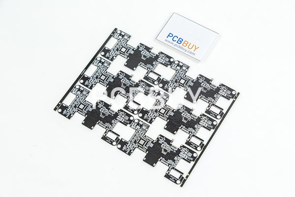
PCB panelization is the process of arranging multiple individual PCB units, often called units or arrays, into a larger manufacturing panel.
Instead of fabricating one small PCB at a time, the manufacturer processes multiple units together through part or all of the PCB manufacturing process.
A panel may contain:
Multiple identical PCBs
Multiple related PCB designs
A PCB array for automated assembly
Tooling areas
Process rails
Fiducials
Breakaway structures
V-CUT lines
Routing paths
Test features
The objective is not simply to fit as many boards as physically possible.
A practical panel must also satisfy manufacturing and assembly constraints.
Why Does PCB Panelization Affect Manufacturing Cost?
At a basic level, PCB manufacturing cost is influenced by how efficiently the manufacturing panel is used.
A simplified conceptual relationship is:
Panel utilization = usable PCB area ÷ total manufacturing panel area
Higher utilization can reduce the amount of unused laminate associated with each finished PCB.
However, this does not mean that maximizing the number of boards on one panel will always produce the lowest cost.
A very dense panel can introduce other costs:
More complicated routing
More difficult V-CUT layout
Additional tooling requirements
Assembly constraints
Increased risk of mechanical damage
Reduced manufacturability
More difficult inspection
Longer depanelization time
Therefore, the cheapest panel is not necessarily the panel with the highest theoretical utilization.
The better target is:
the most efficient panel that remains stable, manufacturable and compatible with the downstream assembly process.
What Are the Main Cost Factors in PCB Panelization?
From an engineering perspective, panelization cost can be divided into several areas.
Panelization Factor | Potential Cost Impact | Engineering Consideration |
PCB dimensions | Material utilization | Optimize board orientation and array arrangement |
Number of units per panel | Processing efficiency | Balance utilization with handling and separation |
Panel size | Material and equipment utilization | Must remain within manufacturing limits |
V-CUT | Separation efficiency | Requires suitable board geometry and spacing |
Routing | Tooling and machining time | Useful for irregular outlines |
Breakaway tabs | Depanelization and edge quality | Must be positioned carefully |
Process rails | Consumes panel area | May be required for assembly |
Board thickness | Affects separation process | Check compatibility with V-CUT/routing |
Layer count | Influences panel capacity | Manufacturing panel dimensions may vary by layer count |
Special processes | May increase complexity | HDI, heavy copper and unusual structures need review |
The important point is that panelization is connected to almost every stage of PCB production.
How Does PCB Size Affect Panelization Cost?
Board size is one of the first parameters to consider.
Suppose a PCB is relatively small.
If the manufacturer can place many units efficiently on a production panel, the unused area can be reduced.
Now consider a large PCB.
Even if the panel is physically large, the number of units that can fit may be limited.
The result is a lower utilization ratio.
This is why a small PCB and a large PCB with exactly the same material and layer count can have very different manufacturing economics.
The panel layout should therefore be evaluated based on:
Board length
Board width
Rotation
Copper distribution
V-CUT direction
Routing clearance
Tooling requirements
Production panel dimensions
What Are the Panel Size Limits at PCBBUY?
According to the current PCBBUY process capability document, the maximum production board dimensions vary with PCB construction.
The published values include:
Single/double-sided boards: 1000 × 600 mm
4-layer: single board up to 1000 × 500 mm, panel up to 1000 × 480 mm
6-layer: single board up to 900 × 500 mm, panel up to 900 × 480 mm
8-layer: single board up to 625 × 500 mm, panel up to 625 × 480 mm
10/12-layer: single board up to 400 × 300 mm, panel up to 600 × 480 mm
The specification also notes that the V-CUT direction cannot exceed the corresponding stated dimension.
This is a useful example of why PCB panelization cannot be separated from layer count.
A panel layout that works well for a 4-layer PCB may not be appropriate for an 8-layer or 12-layer PCB.
How Does V-CUT Affect PCB Panelization Cost?
V-CUT is widely used to separate rectangular PCBs arranged in a panel.
It can be efficient because the separation path is relatively straightforward.
However, V-CUT has geometric and dimensional requirements.
PCBBUY's current capability specifies:
V-CUT board size: ≥75 × 75 mm
Continuous V-CUT cuts require a minimum distance of 2 mm
V-CUT residual thickness is normally one-third of the finished board thickness
Residual-thickness tolerance: ±0.1 mm
V-CUT misalignment: 0.10 mm
Supported V-CUT finished board thickness: 0.4–4.0 mm
The document also states that for thinner boards, such as boards below the normal V-CUT range, stamp holes may be recommended rather than V-CUT.
This has an important cost implication.
If a board is designed specifically for an efficient V-CUT panel, depanelization can be relatively straightforward. If the board outline is highly irregular, V-CUT may not be appropriate and routing may become necessary.
When Should Routing Be Used Instead of V-CUT?
V-CUT works best when the board outline consists primarily of straight lines.
Routing is generally more suitable when the PCB contains:
Irregular contours
Curved edges
Internal cutouts
Complex mechanical profiles
Areas where V-CUT would damage the PCB
However, routing introduces machining paths and therefore requires more consideration of tooling and processing time.
PCBBUY's published capability specifies a standard milling outline tolerance of ±5.2 mil (0.13 mm), with a stated limit of ±2 mil (0.05 mm). The hole-to-edge milling tolerance is listed as ±7 mil (0.177 mm), with a limit of ±4 mil (0.10 mm).
For cost optimization, the key is not to avoid routing at all costs.
It is to use the appropriate separation method for the actual board geometry.

How Does PCB Shape Affect Manufacturing Cost?
Board shape has a direct influence on panel utilization.
Consider three simplified shapes:
Rectangular PCB
Usually easy to arrange and efficient to panelize.
L-shaped PCB
May leave significant unused space around neighboring boards.
Highly irregular PCB
May require routing and larger spacing, reducing panel utilization.
This is why mechanical designers should communicate with PCB engineers early.
A small change in board outline can sometimes improve panel utilization without changing the electrical design.
For volume production, this can have a meaningful cumulative impact.
How Does PCB Orientation Affect Panel Utilization?
Board orientation can significantly influence how many units fit onto a panel.
A PCB may fit four units in one orientation but five units after rotation.
However, rotation must be evaluated together with:
Copper distribution
Component placement
Assembly direction
V-CUT direction
Routing
Fiducial locations
Connector access
Therefore, automatic "best-fit" packing is not necessarily the best engineering solution.
A panelization engineer should optimize the entire production process.
How Does Panelization Affect PCB Assembly Cost?
PCB panelization does not stop at bare-board fabrication.
For PCBA production, panelization can affect:
SMT handling
Conveyor support
Fiducial placement
Solder paste printing
Pick-and-place efficiency
Reflow processing
AOI inspection
Depanelization
If several boards are assembled simultaneously, one PCB panel can pass through the SMT process as one production unit.
This can reduce repeated handling.
However, the panel must be designed around the assembly equipment and component placement. A PCB panel that is excellent for bare-board fabrication may not be ideal for SMT assembly.
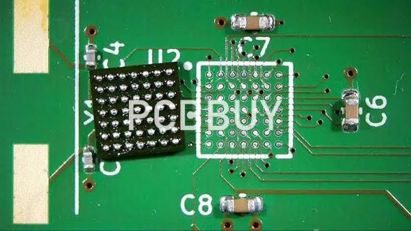
Why Should PCB Panelization Be Designed for Both PCB Fabrication and SMT Assembly?
This is particularly important for automotive, industrial control, power, energy-storage and robotics products.
A typical production chain may be:
PCB fabrication → solder paste printing → component placement → reflow → AOI → functional testing → depanelization → final assembly
If the panelization strategy is optimized only for the first step, downstream processes may become less efficient.
For example, an extremely compact PCB array may leave insufficient space for:
SMT fiducials
Tooling holes
Conveyor support
Edge clearance
Depanelization tooling
The resulting assembly cost can offset any savings achieved during PCB fabrication.
How Should PCB Panelization Be Optimized for Automotive and Industrial Products?
For automotive and industrial applications, I would not recommend optimizing panelization based on material utilization alone.
The panel should be reviewed against:
Electrical requirements
High-current copper
Controlled impedance
Sensitive analog circuits
High-speed interfaces
Mechanical requirements
Mounting holes
Board-edge connectors
Housing constraints
Depanelization stress
Manufacturing requirements
PCB dimensions
Layer count
Copper thickness
V-CUT/routing
Tooling
Assembly requirements
SMT placement
Reflow
AOI
Testing
Depanelization
This becomes particularly important for products such as:
Automotive control modules
Industrial controllers
Power supplies
Battery management systems
Energy-storage systems
New-energy equipment
Motor-control boards
Embodied robotics controllers
How Can PCBBUY Help Optimize PCB Panelization?
PCBBUY's manufacturing capability provides several parameters that should be considered during panelization engineering.
The current process specification supports 1–26 layer PCBs, with production panel dimensions varying according to layer count. For example, the stated panel limits include 1000 × 480 mm for 4-layer panels, 900 × 480 mm for 6-layer panels, 625 × 480 mm for 8-layer panels, and 600 × 480 mm for 10/12-layer panels.
This means panelization can be evaluated against the actual production capability rather than relying on a generic "standard PCB panel."
PCBBUY also supports both V-CUT and milled outlines. The published process capability includes V-CUT dimensional requirements, residual-thickness control and V-CUT misalignment control, while routed outlines have their own dimensional tolerances.
For volume production, this allows the engineering team to evaluate:
PCB dimensions → panel arrangement → separation method → production feasibility
before production begins.
What PCB Panelization Strategy Should You Use?
There is no universal panelization format.
A practical decision can be made using the following framework:
PCB Condition | Recommended Panelization Consideration | Why |
Small rectangular PCB | Dense array + V-CUT where compatible | Good utilization and simple separation |
Medium rectangular PCB | Optimize orientation and array count | Balance utilization and handling |
Irregular outline | Routed panel | V-CUT may not follow the contour |
Very thin PCB | Review stamp-hole or alternative separation | V-CUT may not be suitable |
Heavy copper PCB | Review panel rigidity and separation | Mechanical processing becomes more important |
High-layer-count PCB | Check layer-specific panel limits | Available panel size may change |
Automotive PCBA | Optimize PCB + SMT panel together | Assembly handling and reliability matter |
High-volume product | Optimize utilization and repeatability | Small savings accumulate over production volume |
Complex HDI PCB | DFM review before panelization | Fine features require tighter manufacturing control |
The correct panel is therefore the one that provides the best overall manufacturing balance, not necessarily the maximum nuber of units.
What Should Be Checked Before Finalizing a PCB Panel?
From a manufacturing engineer's perspective, I recommend reviewing at least the following:
1. Unit dimensions
Confirm the exact finished PCB dimensions.
2. Board orientation
Check whether rotating the PCB improves panel utilization.
3. Layer count
Confirm that the selected panel size is compatible with the layer construction.
4. Separation method
Determine whether V-CUT, routing or another breakaway structure is appropriate.
5. Edge clearance
Check mechanical and assembly requirements.
6. Tooling
Determine whether tooling holes, rails and fiducials are required.
7. Assembly requirements
Confirm compatibility with SMT printing, placement, reflow and inspection.
8. Depanelization
Consider how the finished PCB will be separated without damaging components or board edges.
9. Production volume
The optimal panelization strategy for 100 boards may not be the same as that for 100,000 boards.
10. Manufacturer capability
Verify the actual panel dimensions, V-CUT limits, routing tolerances and minimum production dimensions with the PCB manufacturer.
FAQ
What is PCB panelization?
PCB panelization is the process of arranging multiple individual PCB units into a larger manufacturing panel so that they can be fabricated and, when appropriate, assembled more efficiently.
How does PCB panelization impact manufacturing cost?
PCB panelization can affect material utilization, the number of PCBs processed per panel, tooling, routing or V-CUT requirements, assembly handling and depanelization. A well-designed panel can improve overall production efficiency, especially for volume manufacturing.
Does higher PCB panel utilization always mean lower cost?
No. Maximum utilization can sometimes create more complicated routing, difficult depanelization or assembly problems. The best panelization strategy balances material utilization with manufacturing and assembly requirements.
What is the difference between PCB panelization and PCB array?
PCB array generally refers to multiple PCB units arranged together, while PCB panelization is the broader manufacturing process of creating a production panel that may include the PCB array, rails, tooling structures, fiducials and separation features.
Is V-CUT cheaper than PCB routing?
Not universally. V-CUT can be efficient for suitable straight-edge PCB designs, while routing is more appropriate for irregular outlines. The most economical method depends on the board geometry and manufacturing requirements.
What PCB shapes are best for panelization?
Rectangular PCBs are generally easier to arrange efficiently because they can be packed closely and are often suitable for V-CUT. Irregular shapes may require routing and additional spacing.
What is the maximum panel size supported by PCBBUY?
The current published process capability specifies different maximum panel dimensions according to layer count. For example, 4-layer panels can reach 1000 × 480 mm, while 6-layer panels can reach 900 × 480 mm and 8-layer panels can reach 625 × 480 mm under the stated conditions.
What is the minimum panel size supported by PCBBUY?
The published capability states that the minimum conventional single-board size is ≥20 × 30 mm, while the minimum production panel size is greater than 60 × 60 mm. For V-CUT panels, the minimum production size is greater than 80 × 80 mm.
What V-CUT thickness range does PCBBUY support?
The published capability specifies V-CUT for finished PCB thicknesses from 0.4 mm to 4.0 mm. For thinner boards, the document recommends considering stamp-hole structures where appropriate.
What is PCBBUY's V-CUT tolerance?
The published capability specifies V-CUT residual thickness as one-third of the finished board thickness with a tolerance of ±0.1 mm, and V-CUT misalignment of 0.10 mm.
What is PCBBUY's routed-outline tolerance?
The published capability lists a standard milling outline tolerance of ±5.2 mil (0.13 mm), with a stated limit of ±2 mil (0.05 mm). Hole-to-edge milling tolerance is listed as ±7 mil, with a stated limit of ±4 mil.
Should PCB panelization be considered during PCB design?
Yes. For volume products, panelization should ideally be considered during the DFM stage. Board dimensions, outline geometry, component placement, V-CUT/routing, tooling and assembly requirements can all influence the final panel structure.
Does PCB panelization affect SMT assembly?
Yes. PCB panel design can affect solder-paste printing, pick-and-place handling, reflow, AOI, conveyor support, fiducials and depanelization. A panel optimized only for bare-board fabrication may not be optimal for PCBA.
How many PCBs should be placed on one panel?
There is no universal number. The optimal quantity depends on PCB dimensions, production-panel dimensions, layer count, board geometry, V-CUT/routing requirements, assembly constraints and production volume.
Can PCBBUY help optimize the panelization design?
Panelization should be reviewed against the actual PCB dimensions, layer structure and manufacturing requirements. PCBBUY's documented capabilities provide specific production-panel dimensions and V-CUT/routing parameters that can be used during DFM evaluation.
Is PCB panelization important for automotive and energy-storage PCBs?
Yes. These products often combine complex mechanical outlines, thick copper, high-reliability requirements and automated assembly. Panelization should therefore balance production efficiency with mechanical handling, depanelization and quality requirements.
Industry Category








