
How Does PCB Stackup Affect Power Integrity?
By:PCBBUY 09/24/2026 15:24
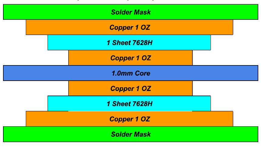
PCB stackup design is often discussed in terms of signal routing, impedance control, and layer utilization. However, it also has a direct influence on power integrity.
The position of power and ground planes, dielectric thickness, copper distribution, via structures, and the location of high-current paths all affect the impedance of the power distribution network (PDN). A poorly planned stackup can increase parasitic inductance and voltage fluctuation even when the power planes appear electrically large enough.
Therefore, understanding how PCB stackup affects power integrity is important for high-performance electronics, particularly in automotive electronics, industrial control, power equipment, energy storage systems, new-energy equipment, and embodied robotics.
From a PCB manufacturing perspective, the challenge is to translate the electrical requirements into a stackup that can also be laminated, drilled, plated, and inspected consistently.
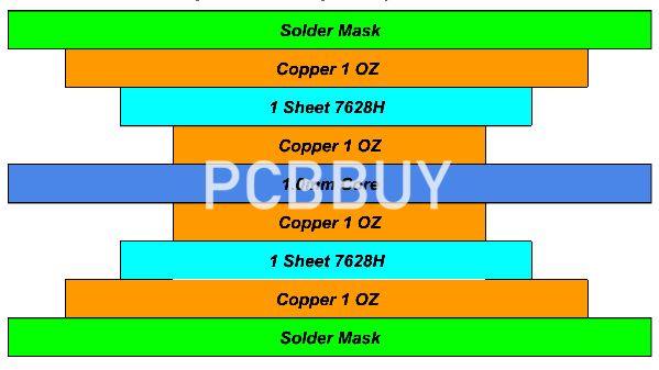
1. Why Does PCB Stackup Matter for Power Integrity?
A PCB power distribution network is not an ideal conductor. It contains resistance and inductance throughout the path from the voltage regulator to the device.
When a device suddenly changes its current demand, the parasitic inductance of the PCB can contribute to transient voltage variation. A simplified relationship is:
V = L × di/dt
The faster the current changes, the more important the inductive component becomes.
The stackup influences this behavior because it determines:
-
The distance between power and ground planes
-
The location of power planes relative to components
-
The length of vertical power paths
-
The available space for power and ground vias
-
The geometry of high-current loops
-
The reference planes available to high-speed signals
-
The location and effectiveness of decoupling capacitors
Consequently, power integrity should be considered when the layer structure is established, rather than being treated as a routing problem after the stackup has already been finalized.
2. How Does Power-Ground Plane Spacing Affect Power Integrity?
One of the most important stackup parameters is the dielectric spacing between a power plane and its associated ground plane.
A closely coupled power-ground pair has lower spreading inductance and greater distributed capacitance than the same planes separated by a thicker dielectric. This can help the PCB provide a lower-impedance path over part of the PDN's frequency range.
However, this does not mean that the thinnest possible dielectric should always be selected.
Very thin dielectric structures can create additional manufacturing and mechanical considerations, including lamination control, resin flow, registration, insulation requirements, and board flatness.
The actual dielectric thickness should therefore be selected according to the combined requirements for:
-
PDN performance
-
Controlled impedance
-
Breakdown and insulation requirements
-
Layer-to-layer spacing
-
Manufacturing capability
-
Overall board thickness
-
Thermal and mechanical reliability
For high-speed boards, the same plane arrangement can also influence signal return paths. A stackup that provides a close and continuous reference plane can reduce unnecessary return-current loops and improve electromagnetic behavior.
3. How Does the Position of Power and Ground Planes Affect Decoupling?
Decoupling capacitors can only work effectively when their electrical connection to the device and power planes has sufficiently low inductance.
If the power and ground planes are located far from the component layer, the current must travel through longer vias and interconnect structures before reaching the PDN.
This additional path contributes parasitic inductance.
Therefore, for critical power rails, engineers should consider the relationship between:
Device → capacitor → via → power/ground planes
rather than evaluating the capacitor alone.
A practical stackup should provide suitable access to the power and ground planes near the components that generate the largest transient current demand. Multiple power and ground vias can also be used to create parallel current paths where layout density permits.
For BGA devices, HDI structures can provide additional flexibility because laser microvias can connect outer-layer circuitry with nearby internal layers without requiring every connection to use a long through-hole via.
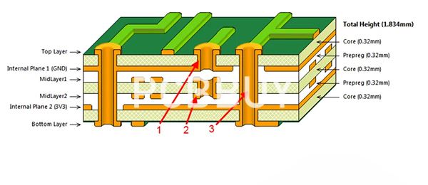
4. How Does PCB Stackup Affect High-Speed Signal Return Paths?
Power integrity and signal integrity are closely related.
High-speed signals require a controlled return-current path. If the reference plane is interrupted by a split, void, or unsuitable layer transition, the return current may need to take a longer path.
This increases loop area and can contribute to unwanted electromagnetic coupling.
For this reason, a good stackup should consider both:
Power distribution paths
and
Signal-and-return paths
A power plane should not automatically be treated as an equivalent substitute for a continuous ground reference for every high-speed signal. The actual layer arrangement and return-current path should be evaluated according to the signal structure.
When a signal changes layers through a via, the corresponding return-current transition should also be considered. Nearby ground vias can help provide a shorter return path where appropriate.
5. How Do Copper Thickness and Layer Allocation Affect Power Integrity?
Copper thickness affects the DC resistance of power distribution structures. For high-current rails, insufficient copper cross-section can increase voltage drop and localized heating.
However, simply making every layer heavy copper is rarely the most efficient approach.
A better strategy is to allocate copper according to the electrical function of each layer.
For example:
-
High-current power layers may require thicker copper.
-
Ground layers may need sufficient copper area for low-impedance return paths.
-
High-speed signal layers may require finer geometries and more controlled copper thickness.
-
Mixed power/signal layers need careful evaluation to avoid compromising either function.
This is particularly important for boards combining power electronics with communication or control circuits.
|
Stackup Factor |
Power Integrity Effect |
Design Consideration |
|
Power-ground plane spacing |
Influences plane capacitance and spreading inductance |
Select dielectric thickness based on electrical and manufacturing requirements |
|
Plane location |
Affects the distance between devices, capacitors, and PDN planes |
Keep critical power paths compact where practical |
|
Copper thickness |
Influences resistance and current-carrying capability |
Use thicker copper where current requirements justify it |
|
Via structure |
Adds resistance and inductance to vertical power paths |
Use appropriate numbers and locations of parallel power/ground vias |
|
Reference-plane continuity |
Influences signal return paths and coupling |
Avoid unnecessary discontinuities beneath critical high-speed routing |
|
Layer symmetry |
Affects mechanical balance and warpage |
Balance copper and dielectric structures during stackup development |
6. Should Engineers Use More Power Planes to Improve Power Integrity?
Adding power planes can provide additional current-carrying capacity and make power distribution easier to manage, but it also increases layer count and can reduce routing flexibility.
Multiple voltage rails can further complicate the design. Splitting planes without considering signal return paths may create new signal-integrity and EMC problems.
The better approach is to determine the required power architecture first and then assign layers according to:
-
Number of voltage domains
-
Current requirements
-
Device placement
-
Decoupling strategy
-
High-speed routing requirements
-
Thermal requirements
-
Manufacturing constraints
For a complex multilayer board, PDN simulation and stackup analysis can be used before final routing to identify problematic impedance regions or resonances.

7. How Should Stackup Design Balance Electrical and Manufacturing Requirements?
An electrically attractive stackup is not necessarily a good production stackup. For example, a design may require very fine HDI structures, multiple thin dielectric layers, heavy copper, and complex mixed-material lamination simultaneously. Each requirement may be technically achievable on its own, but their combination can significantly increase process complexity.
PCBBUY supports customized multilayer PCB fabrication and can manufacture high-layer-count boards within its stated process range. Its HDI capability supports first-order and second-order structures, with laser blind vias down to approximately Φ0.075 mm and mechanical blind vias down to approximately Φ0.15 mm, depending on the complete board structure.
For high-current designs, PCBBUY also supports heavy and partial-heavy copper structures, with capabilities of up to 15 oz copper on outer layers and 8 oz on inner layers, subject to the specific design and manufacturing process.
The maximum supported PCB size is approximately 1000 × 600 mm, which can be relevant to larger industrial, power, energy-storage, and system-level control boards.
These capabilities allow the stackup to be developed around the actual electrical requirements instead of forcing the electrical design into an unsuitable standard board structure.
8. What Quality Controls Should Be Considered After Stackup Design?
Power integrity ultimately depends on the manufactured PCB matching the intended design.
Important manufacturing variables include:
-
Final copper thickness
-
Layer registration
-
Dielectric thickness
-
Hole and via quality
-
Plating consistency
-
Lamination quality
-
Board flatness
-
Electrical continuity
PCBBUY uses inspection and testing processes including AOI, flying-probe testing, and four-wire low-resistance testing.
Four-wire resistance measurement is particularly useful when low-resistance connections need to be evaluated more accurately, while AOI and electrical testing provide additional process-control and verification steps.
For complex multilayer boards, customers should provide the complete stackup, material specifications, copper requirements, impedance requirements, and special via instructions together with the Gerber files. This allows manufacturing engineers to review the electrical design together with its fabrication requirements.

Conclusion
How PCB stackup affects power integrity can ultimately be understood through the relationship between current paths, impedance, inductance, capacitance, and return paths.
Power-ground plane spacing influences the electrical behavior of the plane pair. Plane location affects the connection between the device, decoupling network, and PDN. Copper thickness affects resistance and current capacity, while via structures influence the vertical power path. At the same time, the stackup determines the reference-plane environment for high-speed signals.
The goal is therefore not to create the thickest copper or the largest number of power planes. It is to create a balanced stackup that meets electrical, thermal, mechanical, and manufacturing requirements simultaneously.
For automotive, industrial control, power, energy storage, new-energy, and embodied robotics products, PCBBUY can support this process through multilayer PCB fabrication, HDI, heavy and partial-heavy copper, high-frequency material processing, and electrical inspection capabilities. Early stackup review with the PCB manufacturer can help ensure that the intended power-integrity architecture is not only electrically sound but also practical for stable production.
FAQ
1. How does PCB stackup affect power integrity?
PCB stackup affects power integrity by determining power-ground plane spacing, current-path geometry, via length, plane inductance, distributed capacitance, and the location of the PDN relative to components and decoupling capacitors.
2. Should power and ground planes always be placed next to each other?
A closely coupled power-ground pair can be beneficial for reducing spreading inductance and increasing distributed capacitance, but the exact layer arrangement depends on the complete PCB design. Dielectric thickness, impedance requirements, manufacturing capability, and insulation requirements must also be considered.
3. Does a thinner dielectric always improve power integrity?
Not automatically. A thinner dielectric can improve power-ground coupling, but extremely thin structures may introduce manufacturing and mechanical challenges. The final thickness should be selected based on both electrical performance and PCB fabrication requirements.
4. How does copper thickness affect PCB power integrity?
Greater copper thickness can reduce resistance and improve current-carrying capability. However, thicker copper can also affect routing density, etching, impedance, and manufacturing complexity. Copper thickness should therefore be matched to the actual current requirements.
5. Can HDI improve power distribution in high-density PCBs?
HDI can provide shorter and more flexible vertical connections, particularly around dense BGA packages. PCBBUY supports first-order and second-order HDI structures and laser blind vias down to approximately Φ0.075 mm, subject to the specific stackup and manufacturing requirements.
6. What should be provided to a PCB manufacturer for stackup review?
A complete manufacturing package should ideally include Gerber files, layer count, stackup, material specifications, copper thickness, dielectric requirements, impedance targets, via specifications, board dimensions, and any special power-integrity or reliability requirements. Early engineering review can identify conflicts between the electrical design and manufacturing process before production.
Industry Category








