How Is PCB Inspection Classified according to Different Standards?
By:PCBBUY 05/13/2024 17:22

Printed circuit boards (PCBS) are widely used in a variety of electronic devices, whether it is mobile phones, computers or complex machines, you can find circuit boards. If the PCB has defects or manufacturing problems, it can cause the final product to malfunction and cause inconvenience. In these cases, manufacturers will have to recall the devices and spend more time and resources to fix the fault.
Therefore, PCB testing has become an indispensable part of the circuit board manufacturing process, which finds problems in time, assists the staff to deal with them quickly, and ensures the high quality of the PCB.
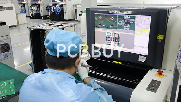
Generally, PCB inspection can be divided into two categories: manual visual inspection, equipment, and instrument inspection.
Electronic Contract Manufacturers (Startsmall tech) offer a variety of PCB test methods, but the seven main types include:
Visual inspection
In-circuit testing (ICT)
Flying probe testing(FPT)
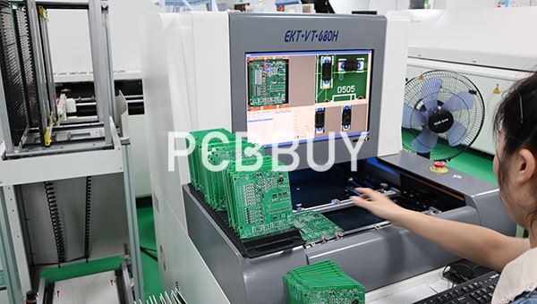
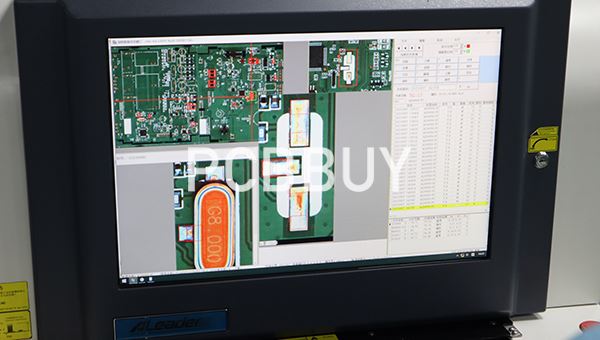
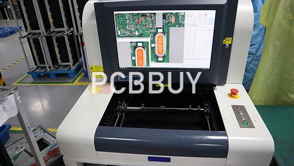
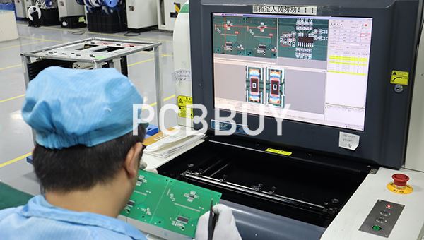
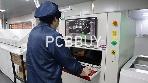
Automated optical inspection(AOI)
X-Ray inspection
Burn-in testing
Functional testing (FCT)
Let’s take a look at the 7 common test methods for PCBs.
What Are the 7 Main Types of PCB Testing during Manufacturing Process?
1. Visual Inspection
Manual visual inspection is still the most widely used test method. It only requires a low up-front cost, no test fixture requirements, and only one operator equipped with a simple magnifying glass or microscope. This test method can be changed flexibly and can be well adapted to product changes.
Therefore, this test method is still widely used in major PCB board factories.
Its main shortcomings are: the detection result is affected by the subjective error of the operator, the training cost is high, and the data collection and sorting are difficult.
At present, due to the gradual development of PCB in the direction of precision, customers have higher and higher requirements for product reliability, and middle and high-end PCB manufacturers began to gradually focus on equipment and instrument inspection.
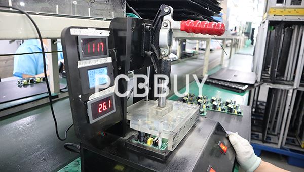
2. IN-CIRCUIT TESTING (ICT)
ICT, or In-circuit testing, is a must-have testing equipment for modern PCB manufacturers. It is very powerful. It provides a reliable, high-fault coverage verification method for all electronic components in PCB components.
It is mainly through the test probe contact PCB layout test point to detect PCBA circuit open, short circuit, all parts of the fault, and clearly inform the staff. Even workers with modest electronics skills can easily deal with faulty PCBs.
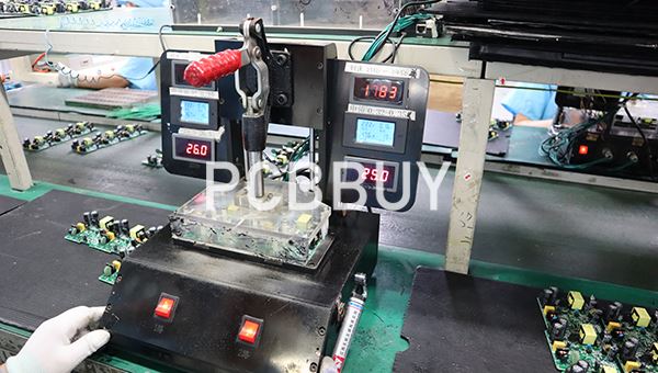
It may be performed with a bed of nails type test fixture and specialist test equipment, or with a fixtureless in-circuit test setup
3. FLYING PROBE TESTING(FPT)
In contrast to traditional testing methods, which place test probes in a fixed position, flying probe testing uses two or more independent probes that operate without a fixed test point (hence the name “flying probe”). These probes are electromechanical and move according to specific software instructions. Therefore, the initial cost of flying probe testing is low, and it can be done by modifying the software without changing the fixed structure.
In contrast, the initial fixture cost of ICT is higher, so flying probe testing is cheaper for small batch orders, but ICT is faster and less error-prone than flying probe testing, so ICT is still more cost-effective for large batch orders.
4. AUTOMATED OPTICAL INSPECTION (AOI)
Automated optical inspection (AOI) is an automated visual inspection of printed circuit board (PCB) (or LCD, transistor) manufacture where a camera autonomously scans the device under test for both catastrophic failure (e.g. missing component) and quality defects (e.g. fillet size or shape or component skew).
It is commonly used in the manufacturing process because it is a non-contact test method. It is implemented at many stages through the manufacturing process including bare board inspection, solder paste inspection (SPI), pre-reflow and post-reflow as well as other stages.
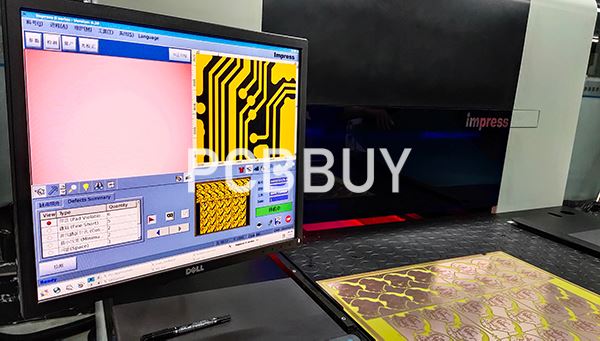
However, AOI will not supply power to the circuit board and cannot detect all components 100%. Therefore, AOI is generally used in combination with other test methods. Commonly used test combinations are:
AOI and flying probe
AOI and ICT
AOI and functional testing
5. X-RAY INSPECTION
X-ray inspection technology, usually referred to Automated X-ray inspection (AXI), is a technology used to inspect the hidden features of target objects or products with X-rays as its source. It is mainly used for the detection of ultra-fine spacing and ultra-dense circuit boards.
Nowadays, X-ray inspection is widely used in lots of applications such as medical, industrial control, and aerospace.
As for PCB inspection, X-ray is massively used in the process of PCB assembly in order to test the quality of PCBs, which is one of the most important steps for quality-oriented PCB manufacturers.
6. BURN-IN TESTING
As the name suggests, the burn-in test is a more intense test of the PCB. It is designed to detect early failures and build load capacity. According to the design requirements, the product is placed under specific temperature and humidity conditions, continuous simulation work for 72 hours to 7 days, record the performance data, reverse the production process for improvement, to ensure that its performance can meet the market demand.
Due to its strength, burn-in testing may destroy the component under test or shorten the service life of the PCB.
7. FUNCTIONAL TESTING (FCT)
Functional testing simulates the actual operating environment and is carried out in the final stages of production as a final quality control procedure. The relevant test parameters are usually provided by the custom.
How to Classify PCB Inspection according to Technology?
1. Classification by degree of automation
(1) Manual detection
Manual detection is a simple printed circuit detection method, its basic principle is under the light, the use of human eyes or optical instruments directly observe the electrical interconnection performance of the printed circuit board manufacturing process, and then compare with the original circuit design, find out the problem of the tested object, and guide the correction of the printed circuit board. Although manual detection is the most direct detection method for printed circuit boards, the detection efficiency is low, and the problem of missing detection is easy to occur, and it is only suitable for simple printed circuit board detection.
(2) Automated detection
In order to improve the efficiency of printed circuit board manufacturing, automated inspection technology has gradually penetrated into all aspects of printed circuit board manufacturing. Automatic detection of printed circuit board is to capture the optical information or electrical interconnection information of the tested object with the help of optical acquisition equipment and mechanical transmission equipment, and then convert it into electrical graphic data through computer equipment, and compare it with the original design circuit graphics, and finally learn the location or problem of the defect of the tested object. Automated inspection shows the advantages of fast and efficient, and is one of the core technologies for monitoring the printed circuit board manufacturing process and managing the reliability of products and materials
2. Classification by detection status
(1) Transient (sampling) detection
In the manufacturing process of the same batch of printed circuits, some objects will be appropriately screened for detection to ensure the stability of manufacturing quality. This detection method is called transient (sampling) detection. Processes such as copper plating and pattern etching for hole interconnects are often inspected with transient (sampling) measurements.
(2) Static detection
Static inspection is one of the main methods to detect the appearance or reliability of printed circuit boards. In the static inspection process, the tested object is fixed, and then the optical device is used to locally observe the area where defects may occur, analyze the performance of the object or measure the size change of the object. Static detection methods are also introduced into the transient (sampling) detection process.
(3) Dynamic detection
The manufacturing and reliability of today's printed circuit board cannot be guaranteed without dynamic testing. Dynamic testing is an on-line testing method based on automation equipment, and its development level is one of the important manifestations of the progress of printed circuit board manufacturing technology. Etching production line is the first process to introduce automatic optical dynamic detection in printed circuit board manufacturing. Through the direct online detection of automatic equipment, the measured etching pattern is compared with the design circuit pattern, and the problem area of the detection object is screened and marked to speed up the repair and manufacturing efficiency of the detection object.
What Is the Standard of PCB Inspection?
Test standardization provides a reliable test guidance method and result determination requirements for PCB testing. Europe, the United States, Japan and South Korea have developed printed circuit board testing standards that meet their respective requirements, such as the International Electrical Industry Commission (IEC) standard, the United States Military (MIL) standard, the International Electronic Industry Connection Association (IPC) standard, the European Union ROHS Directive; China has also promulgated a series of printed circuit board testing standards according to the national conditions, some general material testing national standards (GB) will also be applied in printed circuit board testing, China Electronic Circuit Industry Association has also formulated printed circuit board related standards.
IPC-TM-650 Test Methods Manual developed by the International Electronic Industry Connection Association has the greatest impact on the global printed circuit board industry and is widely used as a standard method for printed circuit board testing.
What Is PCB General Inspection Technology and Application?
Technology and application of appearance magnification inspection
Appearance amplification detection principle
Stereo microscope consists of a common primary objective lens, the two beams after imaging the object are separated by two sets of intermediate objective lens (zoom lens), and form a certain Angle (called the volume Angle, generally 12°~ 15°), and then through the respective eyepiece imaging its magnification change is obtained by changing the distance between the intermediate mirror group, the use of double channel light path, The left and right beams in the binocular tube are not parallel, but have a certain Angle, providing a three-dimensional image for the left and right eyes.
It is essentially two single-barrel microscopes placed side by side, and the optical axis of the two mirrors is equivalent to the viewing Angle formed when people observe an object with two eyes, so as to form a three-dimensional space stereovision image.
A stereo microscope is composed of an eyepiece, an objective lens, a body, a illuminator assembly, a handwheel, a support and a base. According to the actual requirements, the current stereomicroscopes can be selected with a variety of accessories, such as eyepieces and auxiliary objectives with higher magnification if you want to get greater magnification, digital imaging systems can be connected to the computer for analysis and processing through various digital interfaces and digital cameras, cameras, electronic eyepieces and image analysis software. The lighting system also has reflected light, transmitted light lighting, light source halogen lamp, ring lamp, fluorescent lamp, cold light source and so on. These optical principles and characteristics of stereomicroscopes
Metallographic section detection technology and application
In the manufacturing process of printed circuit board, if a quality problem occurs in a certain process, it will lead to the scrapping of the whole board and reduce the yield of the product manufacturing. In addition to the need for finished product testing, semi-finished products or raw materials in the manufacturing process also need to be scaled up. In addition to the conventional magnifying glass inspection, backlight inspection and other detection methods, microcutting (metallographic section) detection technology is widely used by printed circuit manufacturers because of its small investment and wide application range. Metallographic slice inspection is a destructive test that can test the defects and conditions of the surface and sectional microstructure of the printed circuit board, such as resin drilling, coating cracks, hole wall delamination, welding conditions, interlayer thickness, coating quality, etching effect, interlayer adhesion and hole wall roughness.
Metallographic microscope is the most used simple inspection tool in the printed circuit industry, from raw materials to printed circuit products basically need to use metallographic microscope detection. The following is a brief introduction to two metallographic microscope cases.
1. In order to ensure the metallization quality of the printed circuit board, it is necessary to test the roughness of the hole wall after drilling. Drill holes in the test plate with different small drill bits, then complete the sampling and make slices, observe and measure the coarseness of the hole wall with a metallographic microscope. In order to make the measurement more accurate, the sample can be metallized after the hole, then the section is made, and then the condition of the hole wall is observed by metallographic microscopy.
2. In order to ensure the alignment degree of circuit patterns, holes or other characteristic positions between PCB layers, the laminating assistant methods such as target are used. However, due to the influence of the uneven distribution of circuit patterns and the unpredictable fluidity of semi-curing, the interlayer migration will occur during compaction. Therefore, it is necessary to conduct sampling inspection of the printed circuit board to ensure that it meets the quality requirements.
Reference
He Wei, PCB Basic Electrical Information Science and Technology, China Machine Press,373-376
Industry Category


