How PCB Crosstalk Manifests in Design and Manufacturing?
By:PCBBUY 07/25/2024 16:50
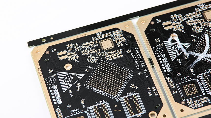
Crosstalk in printed circuit boards (PCBs) is a critical issue that can significantly impact the performance and reliability of electronic systems. This article delves into the phenomenon of PCB crosstalk, exploring its causes, types, effects, and mitigation strategies. With a focus on professional industry knowledge and data, this comprehensive guide aims to provide a thorough understanding of how crosstalk manifests in PCB design and manufacturing.
What is PCB Crosstalk?
Crosstalk in PCBs refers to the unwanted transfer of signals between adjacent conductors or traces, leading to interference and signal degradation. It is an electromagnetic phenomenon where an electric or magnetic field generated by one signal path induces unwanted currents or voltages in another nearby path.
What Is Importance of Understanding Crosstalk?
In high-speed digital and analog circuits, crosstalk can lead to data corruption, timing errors, and overall system instability. Understanding and mitigating crosstalk is crucial for ensuring signal integrity, particularly in densely packed PCBs used in modern electronic devices.
What Are the Types of PCB Crosstalk?
Capacitive Crosstalk
Capacitive crosstalk occurs when a varying voltage in one conductor induces a voltage in an adjacent conductor through the electric field. This type of crosstalk is more pronounced in high-impedance circuits and can affect signal integrity by introducing noise.
What Are the Factors Influencing Capacitive Crosstalk?
Trace Spacing: Closer spacing increases capacitance between traces.
Dielectric Material: The type and thickness of the dielectric material affect the coupling capacitance.
Trace Length: Longer parallel traces increase the likelihood of capacitive coupling.
|
Parameter |
Impact on Crosstalk |
|
Trace Spacing |
Inversely proportional |
|
Dielectric Constant |
Directly proportional |
|
Trace Length |
Directly proportional |
Inductive Crosstalk
Inductive crosstalk occurs due to the mutual inductance between two conductors, where a changing current in one trace induces a voltage in a neighboring trace through the magnetic field. This is particularly problematic in low-impedance circuits and high-frequency signals.
What Are Factors Influencing Inductive Crosstalk?
Trace Width and Thickness: Thicker and wider traces can increase mutual inductance.
Current Flow: High currents can induce stronger magnetic fields.
Loop Area: Larger loop areas between traces increase inductive coupling.
|
Parameter |
Impact on Crosstalk |
|
Trace Width |
Directly proportional |
|
Current Flow |
Directly proportional |
|
Loop Area |
Directly proportional |
Far-End and Near-End Crosstalk
Crosstalk can also be classified based on the location of the induced signal relative to the source:
Near-End Crosstalk (NEXT): Occurs at the end of the line closest to the signal source.
Far-End Crosstalk (FEXT): Occurs at the end of the line farthest from the signal source.
|
Crosstalk Type |
Location |
Characteristics |
|
NEXT |
Near signal source |
More pronounced at lower frequencies |
|
FEXT |
Far from signal source |
Increases with frequency |
What Are the Causes of PCB Crosstalk?
High-Density Designs
Modern PCBs often feature high-density designs with tightly packed traces to accommodate more components in smaller form factors. This close proximity can increase the likelihood of crosstalk.
High-Frequency Signals
As signal frequencies increase, so does the potential for crosstalk. High-frequency signals have shorter wavelengths, leading to more pronounced inductive and capacitive coupling.
Impedance Mismatch
Impedance mismatches between transmission lines and components can cause signal reflections, which may enhance crosstalk effects. Proper impedance matching is crucial in minimizing these reflections.
Poor Grounding and Shielding
Inadequate grounding and shielding can exacerbate crosstalk by failing to provide a proper return path for signals or by allowing electromagnetic interference (EMI) to penetrate the PCB.
What Are the Effects of Crosstalk on PCB Performance?
Signal Integrity Issues
Crosstalk can distort signal waveforms, leading to errors in digital communication systems. This distortion can cause bit errors, reduce data rates, and necessitate error correction measures.
Timing Errors
In high-speed digital circuits, crosstalk-induced noise can alter the timing of signal edges, leading to setup and hold time violations. This can result in data corruption or system malfunction.
Electromagnetic Interference (EMI)
Crosstalk contributes to EMI, which can interfere with the operation of nearby electronic devices and systems. This is particularly concerning in environments with stringent electromagnetic compatibility (EMC) requirements.
Mitigation Strategies for PCB Crosstalk
Layout Techniques
Trace Spacing
Increasing the spacing between adjacent traces reduces capacitive and inductive coupling, thereby minimizing crosstalk. Designers should follow guidelines that recommend specific spacing based on signal frequency and trace geometry.
|
Signal Frequency |
Recommended Spacing |
|
Low Frequency |
3 mils |
|
Medium Frequency |
5 mils |
|
High Frequency |
8 mils |
Differential Pair Routing
Using differential pairs, where two complementary signals are routed together, can help cancel out crosstalk. This method is particularly effective for high-speed digital signals.
|
Parameter |
Differential Pair Benefit |
|
Noise Immunity |
High |
|
Signal Integrity |
Improved |
|
Crosstalk |
Reduced |
Grounding and Shielding
Ground Planes
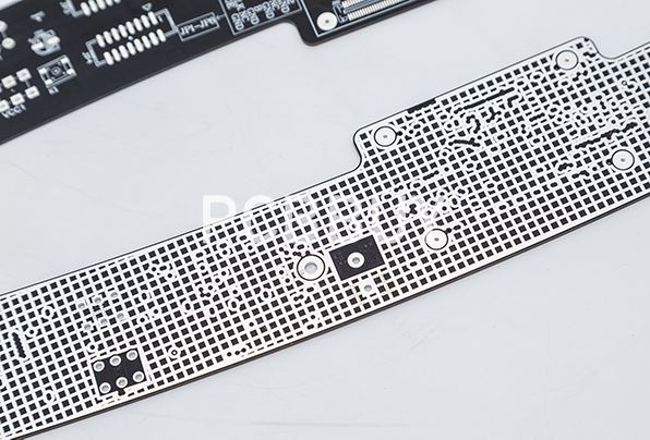
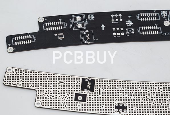
Implementing continuous ground planes beneath signal layers provides a low-impedance return path, reducing inductive coupling. It also helps to absorb and dissipate EMI.
Shielding Techniques
Shielding critical signal traces with grounded metal planes or traces can block electromagnetic fields, preventing crosstalk. Shielding is especially useful in high-frequency and high-density designs.
Use of Guard Traces
Guard traces are grounded or terminated traces placed between high-speed signal lines. They act as a barrier to crosstalk by providing a low-impedance path for induced currents.
|
Guard Trace Width |
Crosstalk Reduction |
|
5 mils |
Moderate |
|
10 mils |
Significant |
|
15 mils |
Maximum |
Termination Techniques
Properly terminating signal lines with resistors or other components can reduce reflections and the potential for crosstalk. Termination techniques such as series, parallel, and Thevenin termination are commonly used.
|
Termination Type |
Application |
Benefits |
|
Series Termination |
High-speed signals |
Reduces overshoot |
|
Parallel Termination |
Matched impedance |
Minimizes reflections |
|
Thevenin Termination |
Complex signals |
Balances DC bias and noise |
Testing and Analysis of PCB Crosstalk
Simulation Tools
Simulation tools like SPICE, HyperLynx, and HFSS are used to model and predict crosstalk in PCB designs. These tools can simulate signal integrity issues and help optimize the PCB layout.
|
Tool |
Application |
Features |
|
SPICE |
Analog circuits |
Circuit-level simulation |
|
HyperLynx |
PCB signal integrity |
Crosstalk analysis |
|
HFSS |
High-frequency design |
Electromagnetic simulation |
Time-Domain Reflectometry (TDR)
TDR is a diagnostic tool used to identify impedance mismatches and crosstalk in PCBs. It measures the reflection of a test signal to analyze the integrity of signal paths.
TDR Parameters
Reflection Coefficient: Indicates the severity of impedance mismatches.
Rise Time: Faster rise times can highlight subtle crosstalk effects.
Trace Length: Provides data on where crosstalk occurs along the trace.
Frequency-Domain Analysis
Analyzing signal behavior in the frequency domain helps identify resonances and frequency-dependent crosstalk issues. Spectrum analyzers and network analyzers are commonly used for this purpose.
|
Analyzer Type |
Application |
Application |
|
Application |
EMI testing |
Identifies interference sources |
|
Network Analyzer |
Impedance analysis |
Measures S-parameters |
Case Studies in Crosstalk Mitigation
Case Study 1: High-Speed Data Transmission
In a high-speed data transmission system, crosstalk was causing significant bit errors. By increasing trace spacing and implementing guard traces, the design team reduced crosstalk by 50%, improving data integrity and transmission rates.
Case Study 2: RF PCB Design
An RF PCB design experienced signal degradation due to crosstalk. The use of ground planes and shielding techniques effectively mitigated the crosstalk, resulting in a 30% improvement in signal clarity and reliability.
Case Study 3: Automotive Electronics
In an automotive electronic control unit (ECU), crosstalk was leading to timing errors and system instability. The implementation of differential pair routing and proper termination techniques reduced these errors, enhancing the ECU's performance.
Conclusion
PCB crosstalk is a complex issue that can significantly impact the performance and reliability of electronic systems. By understanding the causes and effects of crosstalk, designers and engineers can implement effective mitigation strategies to ensure signal integrity. The use of advanced simulation tools, proper layout techniques, and thorough testing are crucial in minimizing crosstalk in PCB product
References
1. M. Montrose, "EMC and the Printed Circuit Board: Design, Theory, and Layout Made Simple," Wiley-IEEE Press, 1999.
2. E. Bogatin, "Signal and Power Integrity: Simplified," 2nd Edition, Prentice Hall, 2010.
3. H. W. Johnson and M. Graham, "High-Speed Digital Design: A Handbook of Black Magic," Prentice Hall, 1993.
4. IPC-2141A, "Design Guide for High-Speed Controlled Impedance Circuit Boards and Assemblies," IPC, 2004.
5. C. R. Paul, "Introduction to Electromagnetic Compatibility," 2nd Edition, Wiley-Interscience, 2006.
Industry Category


