
How PCB Stackup Affects Signal Integrity?
By:PCBBUY 06/30/2026 17:26
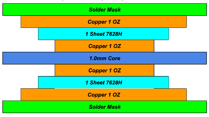
As data rates continue to increase in modern electronics, signal integrity (SI) has become one of the most critical concerns in PCB design. While routing rules and materials are important, PCB stackup design plays a fundamental role in determining signal quality, impedance stability, and EMI performance.
This article explains how PCB stackup affects signal integrity, highlights common stackup-related SI issues, and shows how professional manufacturers like PCBBUY support reliable high-speed PCB production through advanced stackup control.
What Is PCB Stackup?
PCB stackup defines the layer arrangement of copper, dielectric materials, and reference planes within a multilayer PCB. A typical stackup includes:
-
Signal layers
-
Power and ground planes
-
Core and prepreg dielectric layers
The way these layers are arranged directly influences:
-
Characteristic impedance
-
Signal return paths
-
Crosstalk and noise coupling
-
Electromagnetic interference (EMI)
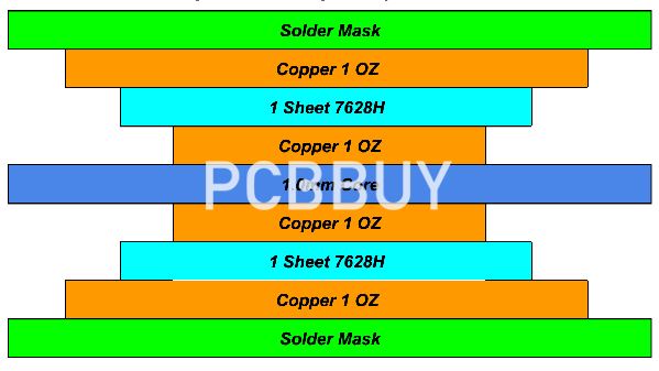
How PCB Stackup Affects Signal Integrity?
1. Impedance Control
Controlled impedance depends on:
-
Dielectric thickness
-
Dielectric constant (Dk)
-
Copper thickness
-
Reference plane proximity
An improper stackup causes impedance mismatch, resulting in:
-
Signal reflections
-
Eye diagram degradation
-
Timing errors at high speeds
2. Signal Return Path Integrity
High-speed signals always require a continuous return path. Poor stackup design can break the return path, leading to:
-
Increased loop area
-
Higher EMI emissions
-
Unstable signal behavior
Dedicated ground planes placed adjacent to signal layers significantly improve signal integrity.
3. Crosstalk Reduction
Stackup symmetry and layer spacing affect both near-end and far-end crosstalk. Proper separation between signal layers and reference planes helps:
-
Reduce capacitive and inductive coupling
-
Improve noise margin in dense routing
Common PCB Stackup Structures and Signal Integrity Impact
|
Stackup Type |
Structure Description |
Signal Integrity Performance |
|
2-layer PCB |
Signal + ground |
Poor for high-speed signals |
|
4-layer PCB |
Signal / GND / PWR / Signal |
Good baseline SI control |
|
6-layer PCB |
Signal / GND / Signal / PWR / GND / Signal |
Very good SI and EMI control |
|
8+ layer PCB |
Dedicated high-speed routing layers |
Excellent SI for high-speed designs |
PCBBUY specializes in 4–26 layer PCB fabrication, enabling optimized stackups for complex signal integrity requirements.
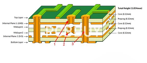
Dielectric Material Selection and Stackup Performance
Dielectric materials within the stackup strongly affect signal loss and impedance stability.
|
Material Type |
Dk Stability |
Loss Performance |
Typical Applications |
|
Standard FR-4 |
Moderate |
Moderate |
General digital circuits |
|
High-Tg FR-4 |
Improved |
Better |
Industrial electronics |
|
Low-loss materials (Rogers, etc.) |
Excellent |
Low |
High-speed, RF designs |
|
Hybrid stackups |
Optimized |
Optimized |
Mixed-signal applications |
PCBBUY supports mixed-material and hybrid stackups, including Rogers and high-Tg laminates, for high-speed signal designs.
Stackup Symmetry and PCB Reliability
Beyond signal integrity, stackup symmetry affects:
-
Board warpage
-
Lamination stability
-
Long-term mechanical reliability
Asymmetrical stackups increase internal stress, which can indirectly impact signal performance through micro-cracking and via reliability issues.
PCBBUY applies balanced stackup principles during DFM review to improve both electrical and mechanical performance.
Stackup Design and EMI Performance
A well-designed stackup:
-
Minimizes loop inductance
-
Contains electromagnetic fields within the PCB
-
Reduces radiation and susceptibility
Poor stackup choices often lead to EMI failures that cannot be fixed by routing alone.
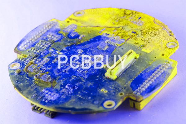
PCBBUY Stackup Design and Manufacturing Capabilities
PCBBUY integrates stackup planning into its engineering and manufacturing workflow.
|
Capability Item |
PCBBUY Specification |
|
Supported Layers |
1–26 layers |
|
Controlled Impedance |
Yes (single-ended & differential) |
|
Minimum Line / Space |
35 μm (1.4 mil) |
|
Dielectric Thickness Control |
Tight tolerance |
|
Material Options |
FR-4, High-Tg, Rogers, Hybrid |
|
Stackup Review |
DFM & impedance simulation |
|
Quality Standards |
IPC Class 2 / Class 3 |
These capabilities ensure that designed stackups translate accurately into manufactured PCBs.
Best Practices for Signal-Integrity-Oriented Stackup Design
To improve signal integrity:
-
Place high-speed signal layers adjacent to solid ground planes
-
Avoid routing critical signals across plane splits
-
Use symmetrical stackups where possible
-
Select materials with stable Dk for high-speed signals
-
Define impedance targets early in the design stage
PCBBUY’s engineering team assists customers with stackup recommendations and manufacturability optimization.
FAQ
Q1: Can routing optimization compensate for poor stackup design?
Only partially. Stackup defines the electrical environment of traces and cannot be fully corrected by routing alone.
Q2: Is a higher layer count always better for signal integrity?
Not necessarily. A well-designed 6-layer stackup can outperform a poorly designed 8-layer PCB.
Q3: Does PCBBUY provide impedance-controlled stackups?
Yes. PCBBUY supports impedance calculation, stackup planning, and controlled impedance manufacturing.
Q4: How early should stackup be defined in the design process?
Stackup should be defined before routing begins, especially for high-speed or differential signals.
Q5: Can PCBBUY manufacture custom stackups based on customer requirements?
Yes. Custom stackups are supported, including hybrid materials and application-specific impedance targets.
Conclusion
PCB stackup design is a core factor affecting signal integrity, especially in high-speed and high-density electronics. Proper layer arrangement, material selection, and impedance control significantly improve signal quality and system reliability.
Industry Category








