How can you be prepared for PCB prototyping to be built?
By:PCBBUY 05/30/2023 14:12

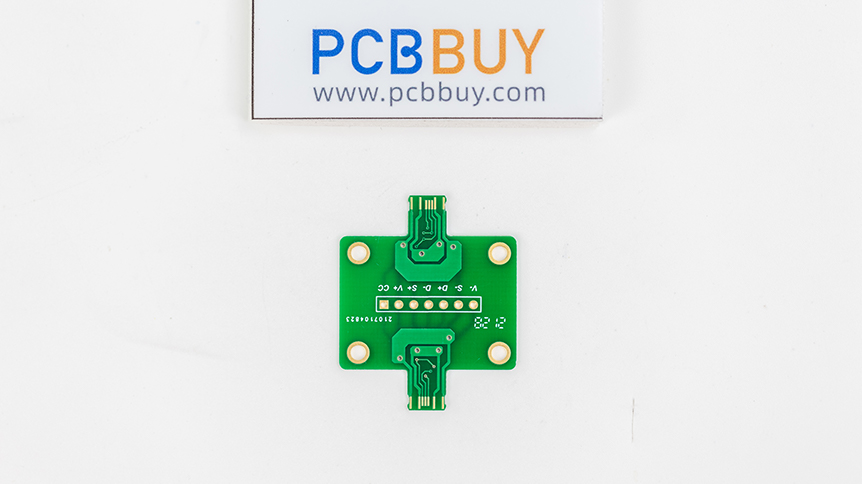
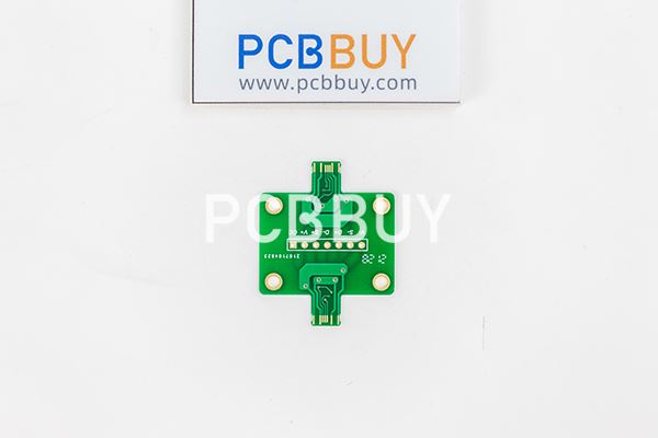
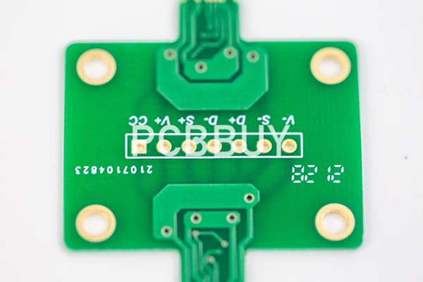
PCB prototypes are early samples of products built with the sole purpose of testing design ideas to see if they work. Although most prototypes, in general, are made to test basic user functionality, engineers require somewhat, if not entirely, functional PCB prototypes to check the complete functionality of designs.
• Detect design flaws early in the production process before you invest significant capital
• Cost-effectively test multiple designs
• Get an accurate portrayal of how your board will function
In this passage, you can get all the basic information about rapid prototyping PCB assembly. If you are looking for the professional knowledge about rapid prototyping PCB assembly, please check and read the content below for more..

How can you be prepared for PCB prototype to be built?
When building a printed circuit board, there are a few things that you should complete before you submit your design for prototyping:
PCB hole size tolerance Proof of concept: A design proof of concept must be fully developed with the circuitry already tested on a breadboard or through simulation. With the circuitry verified on your POC, you’ll spend minimal time testing the prototype, saving on expenses, and possibly additional redesigns.
Ready for manufacturing: Your PCB layout should be complete and ready for manufacturing, including adherence to the design for manufacturing (DFM) requirements. You’ll probably be making board changes to a prototype design to incorporate minor corrections and enhancements, and the last thing you want is to completely redesign the board for mass-production. This would consume more time and expense, and likely require another prototype to re-verify the testing.
Good component choices: Many times a prototype design is rushed through production to test the functionality of the circuitry. Such a choice is understandable but can create problems if care wasn’t taken in selecting the components for the board. For circuit boards that will be mass-produced for a long period, they must have PCB components that won’t be discontinued unexpectedly. Finding secondary market replacements for components that have gone end of life (EOL), or redesigning the board to accept new parts can be expensive and time-consuming.
Complete documentation: Make sure that your PCB design is well-documented for its fabrication and assembly, including a complete bill of materials (BOM). This will mitigate delays or manufacturing mistakes and give the contract manufacturer something to work with if new documentation needs to be generated later.

How to process the PCB prototyping?
Manufacturing is different from designing
The design of your PCB might look good on paper or a computer screen - but it can be an entirely different story when it comes to manufacturing it.
For example, there may not be sufficient tolerances between tracks on the board, which later on in the process could result in the circuit shorting out. Or perhaps the design includes a number of components positioned closely together, each with a different thermal mass. Achieving a quality solder joint on each of these components without heat damaging the rest of the circuit board requires expert process engineering skills.
If you are manufacturing a double-sided PCB, there are other factors to consider. Adopting this approach can allow you to fit more components into a limited space or to keep down costs. However, you will need to ensure that, where possible, your largest components are all placed on one side of the board and that this side is passed through the oven second. Otherwise, you risk these components falling off the board. You can use glue to hold down particularly difficult parts, but this requires additional manual work.

Although the design and manufacturing of a printed circuit board assembly can be generalized as schematic capture, PCB layout, and circuit board fabrication and assembly, the details of each step are very involved. We’ll take a look here at some of the more specific aspects of each of these steps.
Before you can start the design of the board within the CAD tools, you have to make sure that you have the library parts to work with first. For the schematic this means creating logic symbols for the parts that you will be working with; resistors, capacitors, inductors, connectors, and integrated circuits (IC’s). With these parts ready for use, you can then begin to organize them on the schematic sheets within the CAD tools. Once the parts are roughly placed, you can then draw in the lines of connectivity between the pins of the schematic symbols.
Industry Category


