How does flying probe test work?
By:PCBBUY 07/13/2021 09:11

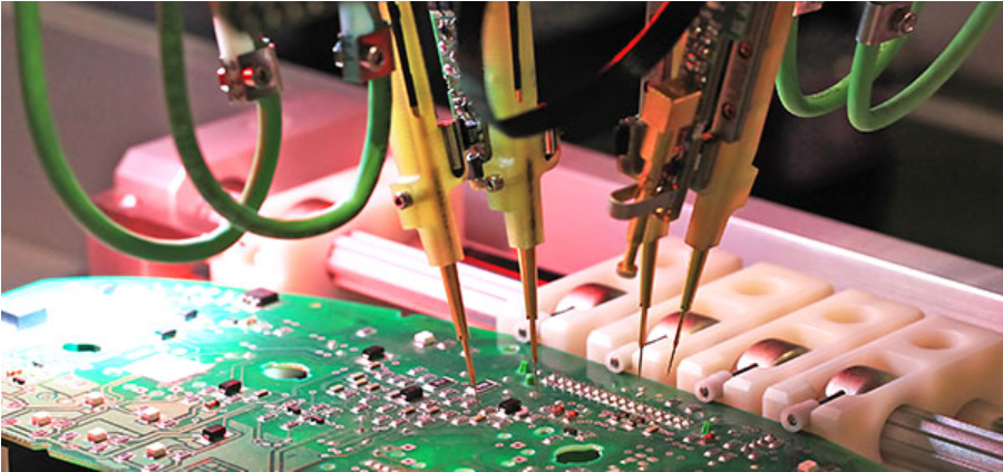
In simple terms, a flying test probe (FPT) is an automated system with a small number of probes that “fly” or maneuver around the top and bottom of a PCB simultaneously to contact test points. According to the instructions in a program for the specific board undergoing testing, a flying test probe moves from one test point to another according to its instructions.
FPT machines have high-precision needles that perform electrical tests to determine if a printed circuit board is in good order. An FPT test does not require custom tooling or manufacturing of a test fixture. That makes it highly cost-effective and the go-to choice for boards in the early development stage and low to mid-volume production.
In this passage, you could learn everything about flying probe test including the working principles of it. Please follow to read the content we prepare.

How does flying probe test work?
Flying probe tests are increasingly becoming popular, especially with the current trend of miniaturizing electronics. Small-sized electronics have small circuit boards that are more cost-effective to test using FPT. Besides, programming complex and dense boards are easier with a flying probe tester.
A flying probe test works fairly straightforward. The steps include:
Step 1:
The first step is to create an FPT test program that will test the circuit board assembly. Developing the test program is generally on an offline PC using an FPT test program generating application. The application needs the PCB assembly’s Gerbers, BOM, and ECAD files. The BOM should be in an EXCEL format, and the ECAD file should be an intelligent CAD file.
Step 2:
After creating the test program, the next step is to load it on the FPT tester. The circuit board assembly that requires testing goes on a conveyor belt inside the tester. The circuit board can be a single board or several boards. The board will travel on the conveyor belt to the area where the probe takes place. The test program controls how the probes contact the pads and the exposed vias.

Step 3:
Next, the FPT applies power and electrical test signals to the probe points and then reads the measurements. Further processing of the measurement readings will determine if a specific circuit portion meets the expected results. Any deviation from set programs and expectations will signal a defect in the unit, resulting in a failed test.
What are the features of flying probe tester?
The flying probe tester comes with adequate AC and DC power supplies, digital multimeters, multiplexing systems, frequency counters, various sensors, and signal generators to animate or excite the PCB nodes and make precise measurements. All these elaborate and intricate connections and signals enable the FPT to isolate component segments currently under test from other interconnections on the board. In other words, the measurement for each component is highly accurate since there are no interferences from the rest of the interconnections on the board. By isolating each component segment, the flying probe tester can measure values accurately.

Perhaps, more interestingly, most FPTs currently available can measure pads of ICs through capacitive probing. Apart from testing for opens, shorts, and other component values, flying probe testers have cameras that check for missing components and inspect each component for polarity. Another test the FPT performs is a diode impendence test to check the inputs of integrated devices.
What are the advanced features of flying probe test?
While all these complex processes are great for ensuring accurate and high-quality tests, a few other emerging advanced features make flying probe tests desirable. These include:
1. Phase Difference Measurement Unit: The PDM unit sends signals to estimate the phase difference between different board sections. This feature reduces the need for isolation tests that are not necessary.
2. High Voltage Stress (HVS) Test: If the PDM misses any high resistance isolation defects, the HVS test will run and apply high voltage to the various test points. Doing so will detect the flaws. 250V is the maximum application voltage in keeping with typical measurements. However, HVS provides a lot more voltage than that. It offers options ranging from 500V to 1000V, and at the same time, it ensures the use of the right amount of power to prevent damages to the boards during high resistance tests.
3. Micro Shorts Detection: It is not uncommon for parts containing micro shorts to burn out due to the application of sudden high voltage. For this reason, micro shorts detection allows the application of low voltages and then increasing it gradually to prevent damages.
In a nutshell, a flying probe test carries out a comprehensive test on the board as much as it is feasible, depending on how easy it is to access a board’s design.
Industry Category


