How to Avoid Crosstalk in PCB Design with Effective Guidelines?
By:PCBBUY 04/08/2022 10:08

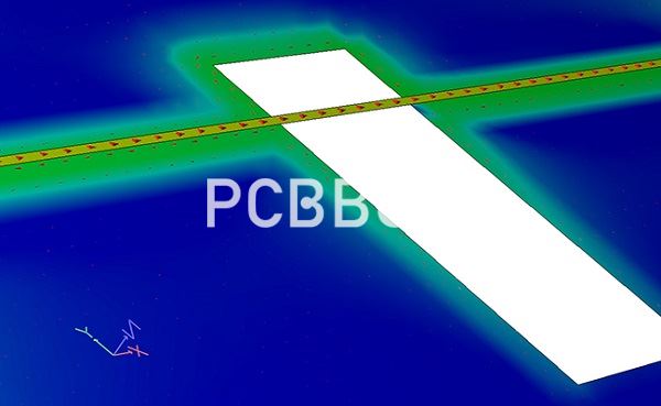
Crosstalk is defined as the unintentional electromagnetic coupling between traces on a printed circuit board. The overpowering of one signal in a trace by another one is the result of this coupling even though the two traces are not in physical contact with each other. This can happen on a PCB that has acceptable trace spacing for manufacturing but where the spacing is not acceptable for crosstalk.
If you are going to learn more information about crosstalk in PCB design, please check and read the content below for professional knowledge.
How to avoid crosstalk in PCB?
So now that you understand a bit about the physics behind crosstalk, how do you guard against it in your PCB designs? The key thing to take away from crosstalk is that it while it occurs everywhere, it’s the largest between parallel signal lines.
The best way to eliminate crosstalk is to exploit the very parallelism that leads to its creation by closely coupling the return path to ground to your high-speed signals. Since the return path is equal in magnitude but opposite in direction, the fields cancel out and reduce crosstalk.
Another way to ensure signal integrity is to use differential signaling, where two voltage lines equal in magnitude but opposite in polarity are used to create a single high-speed data signal. Since the actual data signal is taken as a difference between the voltages of the two voltage lines at the receiver, and because electromagnetic noise tends to affect both lines equally, the signal itself remains perceptible even in the presence of external noise.
· Here’s a quick summary of PCB routing tips for reducing crosstalk:
· Reduce the length that two lines are allowed to run in parallel.
· Be sure to have solid return paths where possible.
· Use differential signaling where applicable.
· Use guard traces with vias connected to ground.
· Keep high-speed signals, especially clock signals, isolated from other traces where possible.
· Keep traces in adjacent layers perpendicular to each other.
What are PCB best practices for avoiding crosstalk?
So now that you understand a bit about the physics behind crosstalk, how do you guard against it in your PCB designs? The key thing to take away from crosstalk is that it while it occurs everywhere, it’s the largest between parallel signal lines.

The best way to eliminate crosstalk is to exploit the very parallelism that leads to its creation by closely coupling the return path to ground to your high-speed signals. Since the return path is equal in magnitude but opposite in direction, the fields cancel out and reduce crosstalk.
Another way to ensure signal integrity is to use differential signaling, where two voltage lines equal in magnitude but opposite in polarity are used to create a single high-speed data signal. Since the actual data signal is taken as a difference between the voltages of the two voltage lines at the receiver, and because electromagnetic noise tends to affect both lines equally, the signal itself remains perceptible even in the presence of external noise.
What is the software of for avoiding crosstalk?
PCB design tools have a lot of functionality built into them to help you to avoid crosstalk in your designs. Circuit board layer rules will help you to avoid broadside coupling by specifying routing directions, and creating microstrip stackups. With net class rules, you will be able to assign greater trace spacing to groups of nets that are more susceptible to crosstalk. Diff pair routers will route your differential pairs together as an actual pair instead of routing them individually. This will maintain the required spacing of the differential pair traces to each other and to other nets in order to avoid crosstalk.
In addition to the built in functionality of your high speed PCB design software, there are also other tools that can help you to eliminate crosstalk in high speed PCB designing as well. There are different crosstalk calculators available to help you determine the proper trace width and spacing for your routing. There are also signal integrity simulators to analyze your high speed design for potential crosstalk problems.
Crosstalk can be a big problem on a printed circuit board if allowed to happen. Now that you know what to look for though, you will be prepared to prevent crosstalk from happening. The design tips that we have discussed here along with the functionality in your high speed PCB design software will help you to create a crosstalk free design.

What are the issues of PCB crosstalk?
Too much activity in a circuit board can make the transmission of a signal difficult. Think of two traces on a circuit board running together side-by-side. If the signal of one trace is “louder” with more amplitude than the signal of the other, it could over-power that other trace. And just as it can be difficult in a noisy room to keep your own thoughts straight when trying to speak, the “victim” trace on a PCB will be similarly influenced by the louder signal. The problem then is that the victim signal will start behaving like the aggressor signal instead of behaving the way that it is supposed to.
Crosstalk is defined as the unintentional electromagnetic coupling between traces on a printed circuit board. The overpowering of one signal in a trace by another one is the result of this coupling even though the two traces are not in physical contact with each other. This can happen on a PCB that has acceptable trace spacing for manufacturing but where the spacing is not acceptable for crosstalk.
Industry Category


