How to Avoid PCB Crosstalk?
By:PCBBUY 03/28/2025 14:20
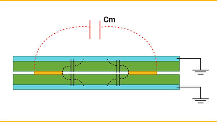
Printed Circuit Boards (PCBs) are fundamental components of modern electronic devices. However, as PCB designs become increasingly complex, they are susceptible to a phenomenon known as "crosstalk." Crosstalk occurs when signals on one trace or wire interfere with adjacent traces, leading to potential performance issues, noise, or system malfunctions. This article explores the mechanisms of PCB crosstalk, its root causes, and effective methods to mitigate it, ensuring optimal PCB performance.
Understanding PCB Crosstalk
What Is PCB Crosstalk?
Crosstalk refers to the electromagnetic coupling between adjacent signal traces or vias on a PCB. It occurs when the electromagnetic field of one signal (the aggressor) interferes with another signal (the victim). Crosstalk can lead to:
-
Signal distortion
-
Increased noise levels
-
Data corruption
-
Reduced signal integrity
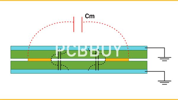
Mechanisms of Crosstalk
Crosstalk arises from two primary mechanisms:
-
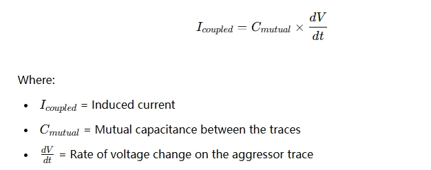
Capacitive Coupling:
-
Occurs when traces are close enough to allow electric fields to interact. The voltage on the aggressor trace induces a current on the victim trace.
-
Formula for capacitive coupling:
-
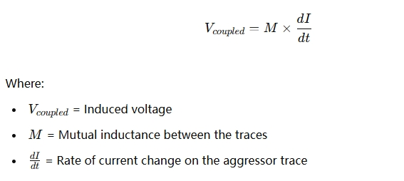
Inductive Coupling:
-
Arises from the shared magnetic fields between traces. Changes in current in the aggressor trace induce a voltage in the victim trace.
-
Formula for inductive coupling:
Types of Crosstalk
-
Near-End Crosstalk (NEXT): Interference measured at the end of the victim trace closest to the signal source.
-
Far-End Crosstalk (FEXT): Interference measured at the end of the victim trace farthest from the signal source.

Factors Influencing PCB Crosstalk
1. Trace Spacing
-
Closely spaced traces increase mutual capacitance and inductance, exacerbating crosstalk.
2. Signal Rise Time
-
Faster rise times lead to higher rates of change in voltage and current, amplifying crosstalk effects.
3. PCB Layer Stackup
-
Improper stackup design can magnify electromagnetic interference (EMI).
4. Ground Plane Design
-
Discontinuous or poorly placed ground planes reduce signal return path efficiency, increasing crosstalk.
5. Differential Signaling
-
Lack of differential signaling for high-speed traces can result in greater susceptibility to interference.
Effective Methods to Avoid PCB Crosstalk
1. Optimize Trace Spacing
Principle
-
Maintain a sufficient distance between traces to reduce mutual capacitance and inductance.
Best Practices
-
Use the "3W Rule": Ensure the spacing between traces is at least three times the trace width.
-
Example:
-
If trace width = 0.2 mm, spacing should be 3×0.2=0.63 \times 0.2 = 0.6 mm.
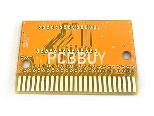
Data Comparison:
|
Trace Width (mm) |
Recommended Spacing (mm) |
Crosstalk Reduction |
|
0.1 |
0.3 |
40% |
|
0.2 |
0.6 |
55% |
|
0.3 |
0.9 |
70% |
2. Use Ground Planes
Principle
-
Ground planes act as reference planes, providing an efficient return path for signals and minimizing coupling.
Best Practices
-
Place ground planes adjacent to signal layers.
-
Avoid splitting ground planes.
3. Employ Guard Traces
Principle
-
Insert grounded guard traces between high-speed signal traces to act as a shield.
Example Design:
-
Aggressor Trace | Guard Trace (GND) | Victim Trace
-
Simulation results:
-
Without guard trace: Crosstalk = 45 mV
-
With guard trace: Crosstalk = 12 mV
4. Optimize Layer Stackup
Principle
-
Proper stackup reduces EMI and crosstalk by controlling trace impedance and ensuring better isolation.
Recommended Stackup:
-
Signal Layer | Ground Plane | Power Plane | Signal Layer
|
Stackup Design |
Crosstalk Risk |
|
2-Layer PCB |
High |
|
4-Layer PCB |
Medium |
|
6-Layer PCB |
Low |
5. Reduce Signal Rise Time
Principle
-
Slower rise times decrease dVdt\frac{dV}{dt} and dIdt\frac{dI}{dt}, mitigating crosstalk.
Implementation
-
Use termination resistors or signal conditioning circuits.

6. Utilize Differential Pair Routing
Principle
-
Differential signals inherently cancel out noise, reducing crosstalk.
Best Practices
-
Maintain equal trace lengths for differential pairs.
-
Example:
-
Differential Pair Trace Length: 10 cm
-
Crosstalk = 5 mV
Advanced Mitigation Techniques
1. Use Advanced Simulation Tools
-
Employ software like ANSYS, HyperLynx, or Cadence for pre-layout and post-layout analysis.
2. Implement Via Stitching
-
Add vias around high-speed traces to connect signal layers to ground planes.
3. Choose Materials with Low Dielectric Constant (εr\varepsilon_r)
-
Materials with lower εr\varepsilon_r reduce signal propagation delay and crosstalk.
|
Material |
εr\varepsilon_r |
Crosstalk Impact |
|
FR-4 Standard |
4.5 |
Moderate |
|
Rogers 4350B |
3.48 |
Low |
|
Isola 370HR |
4.04 |
Medium |
Conclusion
PCB crosstalk can significantly impact the performance and reliability of electronic systems. By understanding the mechanisms of crosstalk and implementing effective design strategies, such as optimizing trace spacing, employing ground planes, and utilizing advanced simulation tools, engineers can minimize its effects and ensure robust PCB functionality. Designing for reduced crosstalk is not only a best practice but a necessity in today’s high-speed, high-density PCB applications.
References
-
Johnson, H., & Graham, M. (2003). High-Speed Digital Design: A Handbook of Black Magic. Prentice Hall.
-
Bogatin, E. (2009). Signal and Power Integrity – Simplified. Prentice Hall.
-
ANSYS Electronics Desktop. (2023). Crosstalk Simulation Tools. [Online]
-
IPC-2141A: Design Guide for High-Speed Controlled Impedance Circuit Boards.
-
Rogers Corporation. (2023). Advanced PCB Material Datasheets. [Online]
Industry Category


