How to Be PCB Designer with 7 Tips for PCB Students?
By:PCBBUY 12/02/2021 09:43

A PCB designer is responsible for taking a 2D schematic and creating the 3D CAD files used to manufacture the PCB. The first step is to create the component footprints, which show the size, shape, and orientation of each component. They develop PCB design guidelines and draft plans for manufacturers that include schematics, assembly, and fabrication drawings. These individuals also identify and resolve mechanical design issues and draft layouts for standard and dense.
Are you a PCB student? Are you going to become a PCB designer? If you are looking for the information about becoming a PCB designer, please check and read the content for more professional information.
What are the contents of a PCB designer?
There are certain skills that many pcb designers have in order to accomplish their responsibilities. By taking a look through resumes, we were able to narrow down the most common skills for a person in this position. We discovered that a lot of resumes listed initiative, speaking skills and writing skills.
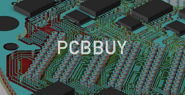
A PCB designer is responsible for taking a 2D schematic and creating the 3D CAD files used to manufacture the PCB. The first step is to create the component footprints, which show the size, shape, and orientation of each component. Second, the PCB designer creates a board outline with the dimensions and shape of the board as well as any keepout areas. Then the components with critical placement requirements are locked down, such as connectors that have to match up with another board.
Once this is complete, the rest of the parts are placed onto the board. Routing is the process of running traces between components to connect them together. Critical routing happens first, where traces that must be the exact same length or traces that must be a specific distance away from another trace are routed first. Then the rest of the board is routed, with traces going up and down through multiple layers of the board. The final task a PCB designer does is to generate all of the manufacturing files.
What kind of education do you prepare for PCB designer?
Many engineers are laying out their own printed boards today. To become an electrical engineer or a mechanical engineer, you will need a BS in those related fields. Traditionally, PCB designers layout the board rather than "engineer" circuit boards or components of the board. As such, the educational background differs some.
For those who are doing PCB layout specifically, there isn’t a degree dedicated to PCB design or printed circuit board creation. You will also find that there are still many positions that do not require the PCB designer to have a degree of any kind. However, you will have much better success as a PCB designer with experience or a degree that includes courses in drafting, computer-aided design, electronic design, hands-on printed circuit board work, or other related areas of study. As PCB designs become more complex, more companies will begin to require degrees for their PCB prototype designers.
There are many printed circuit board certificate courses that are very helpful with the instruction for how to become a PCB designer. Some companies offer specific high speed or multi-layer PCB design and CAD training classes. There is also the IPC Certified Interconnect Designer (CID) course which is an absolute must for the new PCB designer.

What are the responsibilities of a PCB designer?
PCB designers analyze and resolve any design-related issues, provide support to PCB engineering and manufacturing teams, and provide any revisions based on the specifications of customers and engineers.
As mentioned above, a PCB designer is primarily responsible for designing and developing Printed Circuit Boards. They prepare documents for PCB assembly, schematics and fabrications using CAD software and also design layouts to develop high-speed and reliable circuits.
While some PCB designers are in charge of developing the digital or analog designs, others are responsible for working on the routing layout.
These designers review and recommend improvements, if needed, to existing designs and assist various teams in preparing test procedures to verify PCB functions.
· Design and develop Printed Circuit Boards
· Prepare documents for PCB assembly, schematics and fabrications using CAD software
· Design layouts to develop high-speed and reliable circuits
· Develop digital or analog designs
· Work on the routing layout
· Analyze and resolve any design-related issue
· Provide support to PCB engineering and manufacturing teams
· Provide revisions based on the specifications of customers and engineers
· Review and recommend improvements to existing designs
· Assist teams in preparing test procedures to verify PCB functions
Industry Category


