How to Calculate the PCB Component to Component Spacing?
By:PCBBUY 11/27/2023 16:39

PCB Masters choose components early in the design process, realizing that this is the best way to ensure there are no conflicts between the actual design and the components being assembled. If you factor in component sizes from the very beginning, component space and sizes are no longer a concern and the circuit board assembly process can proceed without barriers. This also leads to the next tip.
In this passage we will provide all the information about PCB component to component spacing.
If you are going to learn more about the knowledge of PCB component to component spacing, please check and read the content below.
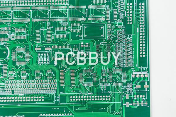
How to Calculate the PCB Component to Component Spacing?
The board designer should talk to the circuit designer and engineers to see if the component size can be reduced, creating additional space on the board. After all, a smaller part will mean a smaller footprint on the board.
Never mix lead-free components with components that are not specified for lead-free assembly. If any component requires lead-free assembly and no substitute for conventional leaded solder is available, then the entire board must be assembled lead-free and all components must be qualified for lead-free assembly.
Sometimes the only package available for a particular device is a lead-free BGA. However, boards that will be used for military projects typically must be assembled with conventional leaded solder, as per government requirements. The designer must either obtain a waiver from the customer to allow lead-free assembly; modify the design to use a device that is available in a package for assembly with conventional leaded solder; or have the BGA reballed for leaded solder (an expensive procedure that can damage parts).
What Is the Purpose of IPC Component Spacing Guidelines?
The IPC component spacing guidelines exist for two reasons: to prevent component overlap that could cause physical damage and to prevent electrical interference that could cause performance problems. Of the two, physical overlaps are a simpler problem to correct. CAD software can catch most instances, and many designers have enough knowledge to identify when components can’t fit in a space without computerized help.

The IPC component spacing guidelines are a third check on these potential physical problems. As long as designers follow the spacing guidelines, there should not be physical overlaps of components except in special circumstances that require additional engineering and development.
Component spacing guidelines also manage negative space—the places where components are not present. Negative space on a PCB can be just as important as the regions where components exist, and this space is particularly important when preventing electrical interference. If conductive traces or circuits are too close together, unintentional connections may form between them as electrons jump between circuits. These unexpected connections reduce the strength of signals traveling through some regions of the PCB and can increase the amount of power flowing through other areas. Reductions in power can cause shorts or failures, while surges in power can cause physical damage or overloads.
What is the importance of PCB component-to-component spacing?
Placing the components on your printed circuit board design is the key to creating a PCB that performs as expected. Bypass capacitors must be close enough to their associated devices to provide an immediate reservoir of power and reduce parasitic inductance between them. Schematic signal paths must be recreated in the layout by placing the components precisely so that the high-speed signals can travel the shortest distance possible between pins. The placement must also be organized so that critical routings doesn’t cross split power planes and thereby lose their return paths.

These are important considerations for designing a successful high-speed printed circuit board, but as we said, there is a balance that must be maintained as well. Parts that are placed close together for performance may end up impacting the ability of the contract manufacturer to easily assemble the board. This may result in added time and cost, or at worst, costly redesigns. To avoid manufacturing problems like these, there are some things you can do with your component placement to help ensure the success of your PCB assembly.
Industry Category


