How to Check PCB Quality with 7 Effective Methods?
By:PCBBUY 12/30/2021 09:32

Printed Circuit Boards are the most used and basic assembly unit applied by all types of electronic devices. All functions and performance of devices are implemented mainly by PCBs. PCB is the heart of electronic devices and both their quality and reliability is directly correlated with quality and reliability of electronic equipment. Nowadays, intelligence and miniature of electronic devices leads to increasingly smaller size and complicated structures of PCBs.
How to check the quality of PCB during the whole manufacturing process? If you are curious about it, please check and read the content below for more information.
1. Confirm the quality of PCB
PCB designers have to check and confirm the design drawings that will be applied by manufacturer for many times prior to manufacturing. Since PCB design can't be successful just after one trial and modifications have to be made time and time again, PCB manufacturers will hold multiple versions of design drawings. So it's necessary to carefully check and confirm the final design drawing provided by manufacturer prior to practical manufacturing so that manufactured PCBs conform to requirement of the last version.
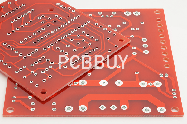
2. Inspect Traces in your PCB Design
Traces are wire conductors responsible for current flow from one component to another. In your PCB- the solder masks cover up the particles. A good practice to reduce errors is color-coding the masks. Traces of only the top and bottom layers of your PCB designs are visible. The usual solder mask color is green- although other colors are also available. White is difficult to notice.
Errors due to Trace misplacement are common. The usual golden rule is- Keep the trace connections as clean as possible. Traces with sharp bends can be problematic for higher power or frequency transmission. Try to avoid steep 90-degree angles. There are exceptions to this general rule too. PCBs with square concentric spirals are a perfect example. We can find these characteristics of high-quality PCB.
3. AOI to check the PCB quality
Typical AOI inspection technologies currently used in circuit board manufacturing include: film inspection, drill inspection, hole location inspection, circuit inspection, blind hole inspection, bump inspection, visual inspection, etc.
At present, the most used AOI inspection technology in the circuit board manufacturing industry is the inspection of the appearance of the circuit board. Although the size of the circuit characteristics of the circuit board has been reduced by more than ten times, the optical system and the matching hardware and software systems have also made great progress.
4. CAF resistance in PCB
Conductive Anodic Filament (CAF) has been increasingly concerns on printed circuit boards in the last few years. The major factors are current trend toward smaller size, lighter weights, thinner and higher performances that the density of PCB shall be designed with more closely spacing conductors, much smaller pitches and single-ply dielectrics such as mobile telephones, notebook computer and camcorder. In the other hand, some electrical applications must be exposed in extreme environment. For example, the safe necessity of automotive like engine control and brake control system. There cannot occur electrical shorts phenomenon, so the insulation resistance of material becomes very importance. These factors are pushing the demand for anti-CAF materials.

5. Requirements of PCB assembly
PCBA quality will depend on your CM’s manufacturing process, especially its adherence to industry standards. And while PCBA performance and reliable operation are primarily design issues, structural integrity and component mounting—as well as the mechanical ability of your boards to remain intact over their projected operational lifecycle—are CM responsibilities that define board quality and contribute significantly to operational reliability.
Be sure to include the board revision and other identifiers, such as publishing date, that clearly distinguish this design. Specify any components or areas of your board that need special attention—for example, polarization, moisture sensitivity and keep-outs. Ensure that any process or readability requirements for silkscreen layer reference indicators, labels and markings are included.
6. Process in-circuit testing
In-circuit testing (ICT) is the most robust type of PCB testing in existence. The high price reflects that -- tens of thousands of dollars, though the cost will depend on board and fixture size, among other factors.
An ICT, also known as a bed-of-nails test, powers up and actuates the individual circuitry on the board. In most cases, the test is designed for 100% coverage, but you’ll get closer to 85-90% coverage. The nice thing about ICT is that the 85-90% you get is totally free of human error.
This test involves using fixed probes laid out in a way that matches the design of the PCB. The probes checks the integrity of the solder connection. The bed of nails tester simply pushes the board down on the bed of probes to start the test. There are access points predesigned in the board that allows the ICT testing probes to make connections with the circuit. They put a certain amount of pressure on the connection to make sure it stays intact.

7. Considerations of FPGA PCB design
I’ll assume you have a rough idea of what external parts you need, as they will be highly dependant on what you are trying to accomplish with your design. In addition to design-specific information, there are a few standards external requirements such as programming interface, communications, and power. This article will briefly cover some of these external requirements, but the concentration of this article is how to physically lay-out the FPGA board at a reasonable cost.
Assuming this design will be either a prototype run or possibly a small production run, it makes sense to design your PCB with specific requirements in mind to keep costs reasonable. The two PCB specifications you are most commonly told are the minimum “trace/space” (that is, minimum width of a trace, and minimum spacing between copper features), and the minimum drill size.
Industry Category


