How to Deal with Technological Developments in PCB Industry?
By:PCBBUY 01/24/2025 14:01

Optimize PCB Equipment
Development Prediction of PCB Equipment
Drilling processing equipment
Drilling processing equipment in the lamination method of multi-layer printed circuit board through the hole processing technology, the use of laser equipment for processing, has been more than 20 years of practice. In 2000, the emergence of dual-beam light CO, the development of optical drilling equipment this technology, so that the laser processing hole speed reached 1000 holes /s, than the initial laser drilling machine hole formation speed increased by about 10 times.
At present, the development of new laser drilling machines continues to move in the direction of higher speed processing. Using CO, laser drilling for hole processing aperture limit of 30 ~40 m. With the development of more refined printed circuit boards, it is predicted that after 2022, UV laser equipment suitable for 20-50 m aperture processing will expand its range of use. In the manufacture of printed circuit boards that require aperture processing in the range of 30 to 40 m, there will be cO, laser drilling machine as the first, and UV laser drilling machine as the second.

At present, the continuous development of multi-layer printed circuit boards containing filled holes with apertures below 50 um, the shape of the plating process holes and the guarantee of the thickness of the insulation layer are more closely dependent on the physical properties of the substrate material. It is predicted that in the next few years, in the substrate materials and later engineering, there will be new solutions to the above topics, and new substrate materials will also appear. In this way, laser drilling opportunities face another important issue, that is, how to cooperate with the new substrate material to achieve high accuracy in the position of the hole, the high precision here refers to the accuracy control in the range of a few microns to 10um.
In terms of mechanical drilling equipment, the practical application of the ultra-high speed spindle of 250,000 /min has promoted the progress of mechanical drilling technology. It is predicted that extremely thin copper foil will be used to process multi-layer printed circuit boards and double-sided printed circuit boards with aperture above 100 um to improve hole quality and improve production efficiency as the main goal, and mechanical drilling technology will have great changes.
Laser equipment
This transformation is directly in competition with laser processing methods with machining apertures below 100 m. In this technical competition, mechanical drilling equipment in the processing of 200 pm aperture, narrow spacing, 150 ~200 m aperture requirements, must solve the problem of improving the quality of processing holes, improve production efficiency, improve metal ion migration resistance and other aspects. One of the important ways is to use high speed to reduce the cutting load.
It can be expected that with the advancement of the technical development of ultra-high speed spindles, the machining of the aperture of 50 ~70 um can be achieved by using mechanical drilling methods.
Due to the appearance and maturity of thin copper foil surface treatment technology, CO is directly used in double-sided printed circuit boards, and the processing of 70 ~100 m through holes by laser drilling machine has become a reality, and after hole processing, the drilling dirt formed by laser drilling at the hole is generally removed. In the future, with the development of laser drilling equipment technology and the application of substrate materials suitable for laser drilling, the processing equipment of the post-processing process of the drilling process with a aperture below 50 um will be reduced, mainly by using UV laser machines. At present, the further development of the laser drilling equipment is mainly around the requirements of coordinating the quality of the hole and the processing speed.
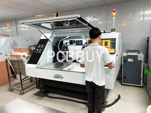
It is predicted that after 2022, there will be a trend of coexistence of laser machining holes and mechanical holes below 50 n. In the way of printed circuit board shape processing, in the future for a long period of time, it is still mainly based on groove processing. In the shape processing of thin plates below 0.2mm, more suitable laser processing methods will be used in the future.
Development of High Density and High Frequency
The development of high-speed and high-frequency electrical signals of electronic products in electroplating equipment has made the wire size control requirements of printed circuit boards more stringent. The purpose of size control is to improve the accuracy of the wire in the aspects of uniformity, smoothness, small size deviation of the upper and lower parts (that is, small side corrosion), small deviation of the thickness of the copper precipitation. In order to achieve excellent accuracy of the wire of 20 ~30 m width, it is necessary to adopt a new process technology different from the traditional electroplating. In this regard, the homogenization technology of coating thickness is very important. In the manufacture of 30 um wire wide circuit graphics, semi-addition method (SAP) or improved semi-addition method (mSAP) is the mainstream.
In order to advance this technology, innovations in etching and electroplating equipment have emerged: the improvement of etching devices combined with the reduction of etching depth; The use of positive and negative pulse rectifier of electroplating equipment: the use of horizontal electroplating equipment, the use of vertical continuous electroplating equipment: the use of special jet mode. Due to the rapid development of the technology of filling holes in high-density multi-layer printed circuit boards, a new topic has been proposed for the manufacturing technology of electroplating equipment.
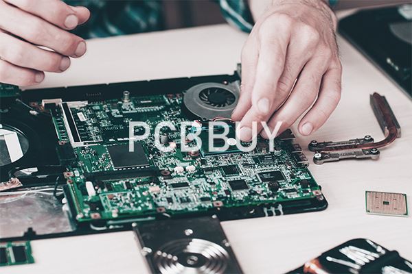
Electroplating has become a major method to fill holes with copper metal. Now the aperture of the filling hole has achieved a fine degree of 45 m, and the number of filling holes is also increasing. In this plating implementation, the problem of copper precipitation should be controlled, and special plating equipment and plating solution should be used for this purpose. In order to achieve high quality and high process stability of electroplating filled holes, it is necessary to increase the number of layers of printed circuit boards in electroplating equipment, plating solution conditions, additives, and brightening agent electrolytic conditions, according to the needs of high-speed circuit development.
High-speed multi-layer printed circuit boards and other aspects of the improvement. The thickness is 3.2~6.0mm, the aperture is generally 0.2 ~0.4mm, and the hole thickness to diameter ratio of the plate reaches 12 ~16, or even 18. The electroplating equipment used in the manufacture of high-speed multi-layer printed circuit board faces the following problems in the improvement of technology: make copper ions can be supplied continuously; The homogenization of the thickness of the precipitated copper film can be achieved in electrolysis: electrolytic conditions, plating solution concentration conditions, additives in order to reduce environmental pollution.
On July 1, 2006, the European Union officially issued and implemented the "Directive on the restriction of the use of certain harmful ingredients in electronic and electrical improvement and other equipment", which has been fully used in the printed circuit industry. For printed circuit boards using lead-free solder, in order to ensure the long-term stability of the connection strength between the circuit layer and the component, heat resistant solder is treated on the final surface of the printed circuit board. The surface treatment of this copper foil can be treated by electroless nickel-gold (Ni-Au) or electroless nickel-gold (Ni-Pd-Au) treatment, electroless tin (Sn) treatment, and electroless silver (Ag) treatment instead of tin-lead (SN-Pb) solder. Implement binary electroplating (Sn-Zn, Sn-Ag, Sn-Cu), ternary electroplating and components
Development of Exposure Equipment
In terms of exposure equipment, whether the above-mentioned subtraction process or addition process to manufacture fine wires, the electrode treatment of the line in the future. A wide width of 30 um will be widely used. For exposure technology, it is necessary to improve the equipment accordingly, and the alignment accuracy of exposure needs to be higher than in the past. In terms of exposure methods, more direct laser imaging will be used.
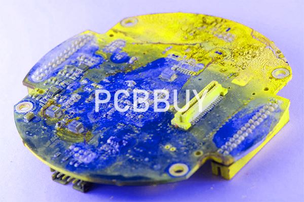
Especially in the manufacture of multilayer printed circuit boards by layering method, the high straightness of exposure equipment to achieve higher precision has become a key research object. Many exposure equipment manufacturers have carried out research in many aspects. For example, X-ray irradiation is used to mark the bottom layer as the target and direct the through hole. soldermask on the copper surface and measure the mark on the lower layer over the insulating resin layer; 3 The use of reflection lighting method to measure the through hole after electroplating processing to determine the advantages and disadvantages of the first white, their development prospects mainly depend on how to overcome its shortcomings.
Adapt to the development trend of high current and high heat dissipation requirements The rapid development of new energy vehicles and 5C communication technology has a great demand for high current and high power transmission. The printed circuit board for high current transmission first needs to meet the design requirements, that is, the product must have good electrical mutual and insulation performance. Therefore, higher requirements are put forward for the manufacturing process of printed circuit board.
Specific Performance in the Following Aspects
1. Manufacturing process development trend
CAF can barely accept it. However, on the printed circuit board with strong current transmission, any CAF phenomenon can not be connected to the high current will inevitably cause the printed circuit board to heat up. At high temperatures, the mismatch of thermal expansion coefficient between multi-layer polyphase materials of printed circuit boards will lead to product stress, which will lead to product reliability problems. Therefore, in the printed circuit board manufacturing process, it is necessary to fully release the stress of the product. Of course, in the design, it is necessary to simulate and design the material selection and diversion structure to ensure the reliability of the printed circuit board.
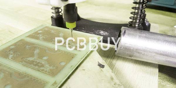
In the case that the printed circuit board itself cannot directly dissipate heat, the use of external media to force heat dissipation (such as copper blocks embedded in the printed circuit board or copper blocks installed on the surface) has become the main solution. Copper block embedding involves a new copper block embedding manufacturing T art. As the printed circuit represented by 5C communication has higher and higher heat dissipation requirements, the process of embedding copper blocks or installing copper blocks will become the mainstream of the manufacturing process of printed circuit boards.
In addition, in some more extreme cases (such as electric vehicles carrying hundreds of amps), the printed circuit board line needs to be several millimeters thick. Conventional line etching technology can not be realized, the use of copper blocks directly cut to form lines and then laminate with resin to make printed circuit boards will become an important direction of future development.
2. Material technology development trend
The thermal conductivity of the printed circuit board substrate is only about 0.2 w/ (m·K). Rapid heat dissipation under high current transmission puts forward new requirements for the heat dissipation of printed circuit board itself. Therefore, improving the thermal conductivity of dielectric materials in printed circuit boards has become a future development trend. At present, the main heat dissipation media for printed circuit boards are Al,0, and Si, fillers. Increasing the thermal conductivity can increase the content of the filler, but it will affect the physical and chemical properties of the printed circuit board.
At present, the focus of material research is on the directional arrangement of fillers to increase the heat dissipation performance. Since the printed circuit board mainly dissipates heat in the Z direction, the thermal conductivity can be improved without increasing the packing as long as the packing is oriented in the Z direction, as shown in Figure 20-10. At present, the technology has been more successful in Japan, and it has begun to carry out industrialization stage in China, and many scholars have begun to study in this field, and achieved good results.
In addition, the improvement of thermal conductivity of dielectric materials is also an important direction. By improving the crystallization property of epoxy resin, a mesomorphic structure can be formed, which can greatly improve the heat dissipation property of resin material. At present, through the combination of mesocrystal resin and filler directional arrangement, the thermal conductivity of the substrate material can be as high as 10W/(m·K), which can greatly solve the problem of heat dissipation caused by high current transmission of the printed circuit board. Although the new material is still in the research and development stage, with the increasing demand for printed circuit boards to replace cables for current transmission, high-thermal dielectric materials are not far from commercialization.
Development Forecast in Response to Greening Requirements
1. Greening problem
The greening problem of environmental protection as the essence of environmental protection issued and implemented by European-centered environmental protection laws and regulations (called "environmental harmonization problem" in Japan) is actually not only a technical problem, but also an economic and social problem. In recent years, the electronic installation industry and the printed circuit board industry have been debating two specific issues: "When to fully implement" (timeline) and "direction of material development." In terms of the enthusiasm (or degree) of the attitude towards the "green" of electronic products, there are differences in various countries and regions in the world. The analysis of this problem, the Japanese printed circuit and substrate materials of the famous expert Mr. One Aoki Masamitsu recently proposed: in the United States, that the 21st century "key industry" is "IT" industry; In Europe, the "key industry" of the 21st century is the "environment". Europe is the "birthplace" of green electronic products. In terms of printed circuit boards, they mainly carry out the process of greening around three aspects. These three aspects are "lead-free", "halogen-free" and "recycling of products".
This is the policy to be adhered to in the future, and through the establishment and implementation of regulations to promote this work. Related to the environmental protection regulations of printed circuit boards, there are two main directives in Europe, namely, the Waste Electrical and Electronic Equipment Directive (WEEE Directive) and the Directive on the restriction of the use of Certain harmful components in electrical and electronic equipment (RoHS Directive). In these two directives, it is mentioned that the use of lead and halides should be banned. It was adopted in October 2002 at a meeting on corporate governance and was fully implemented on July 1, 2006. The release and implementation of these two "European directives" will inevitably have a profound impact on the greening of PCBS in countries around the world.
2. Development and application of halogen-free substrate materials
According to the most common statistics on the use of halogen-free substrate materials in the world, in 1999, the use of halogen-free substrate materials in the world accounted for about 3% of the total use of substrate materials, and the use of halogen-free substrates has increased rapidly in recent years. Due to the implementation of the above two directives (WEEE, RoHs), the use of halogen-free substrate materials in the world has increased to more than 80% of the total substrate materials, and will grow rapidly in the next period of time.
The development of halogen-free substrate materials, in addition to solving the environmental requirements, but also to solve the problem of meeting the performance requirements, to meet the next generation of high-density installation required by the electrical and mechanical properties of the reliability requirements; But also to meet the requirements of mechanical drilling, laser drilling, copper wiring and substrate material bonding, corrosion resistance and many other aspects of the substrate processing performance. It is more difficult to develop than the structure of halogen-free electronic products. According to the different uses of various printed circuit boards, the requirements for the performance of substrate materials are also different, so it is necessary to treat them differently when developing halogen-free substrate materials. For this reason, halogen-free substrate materials can be divided into the following three categories.
What Are the 3 Types of Halogen-free Substrate Materials of PCB?
The development and application of halogen-free substrate materials for general substrates
Such materials are mainly used in general substrates such as household appliances and computers. At present, halogen-free substrate materials on the market are mostly halogen-free substrate materials for general substrates, and epoxy resin as the main component is the mainstream of such substrates. Its main performance characteristics are low cost, high processing interchangeability, high performance stability, and relatively low transmission rate (under 500MHz). At present, the halogen-free substrate materials used for this kind of substrate are mainly composed of cross-linked (that is, reactive) organ phosphorus and metal hydroxide and oxide fillers.
It can achieve high creepage resistance and UL94 VO grade standard requirements due to the addition of organ phosphorus in high humidity environment copper wiring will be corroded, this corrosion phenomenon with the amount of phosphoric acid in the flame retardant becomes more serious. At present, there are different views on the safety of organophosphorus (it contains thermal decomposition products), and it is an urgent problem to verify its safety as soon as possible.
The development and application of halogen-free substrate materials for large high-layer substrates
This kind of material is mainly used in high-speed data storage management computers, communication transmitter devices and other large high-layer substrates. Large high multilayer substrates have high electrical properties with low dielectric constant (35) and low dielectric loss factor (tan 0.005) required for high-speed signal transmission, as well as high T properties (T200C) and low water absorption (<0.3%) required for thermal shock resistance in high temperature lead-free welding installations. Therefore, the resin used in this kind of substrate material is composed of polyphenyl ether resin (PPE), cyanate resin (CE) and its modified resin (BT), polytetrafluoroene grease (PTFE), etc., or the above resin is composed of epoxy resin modification.
Halogen-free substrate materials for large high multilayer substrates, flame retardants used in development, currently using organ phosphorus as the main material. In this way, the contradiction between the high electrical and physical properties to be achieved and the flame retardant properties to be achieved will be more prominent than the development of halogen-free substrate materials for general substrates, which also makes its development work more difficult. Recently, some manufacturers have used flame retardant metal oxides as high-filling micro-fillers to solve the above problems and obtained certain results.
In terms of the recycling development of substrate materials, fluorine resin substrate materials, as substrate materials that have been used in high-frequency electronic products, are the most promising ones to achieve recycling first.
The development and application of chemical free substrate materials for flexible substrates
With the continuous acceleration of the development of flexible substrates, the importance of flexible substrates in the entire electronic substrate is more prominent. At present, the mainly used polycot imides resin film and the liquid crystal polymer (LCP) film that has come out and begun to be used in recent years, which is itself flame retardant. 461 It is expected that due to the development of recycling in substrate materials in the future, thermoplastic liquid crystal polymers (LCP), which are easy to recycle, will receive more attention. In addition, the substrate used for embedded components such as mobile phones and high-frequency modules is also expected to choose a substrate material such as liquid crystal polymer and other thermoplastic resins in the manufacturing, which can solve the recycling problem. In terms of the formation of the insulation layer of printed circuit boards, many new processes are being developed, such as the formation of the insulation layer on the substrate through printing, inkjet, and other processing methods. The insulating materials used in these new ways are considered to be recyclable, and thermoplastic resins such as liquid crystal polymers are used in large quantities.
Reference
He Wei, PCB Basic Electrical Information Science and Technology, China Machine Press,456-461
Industry Category


