Define a PCB Stackup: Comprehensive Guide to PCB Layer Structure
By:PCBBUY 12/02/2021 09:23
Introduction: What Does "Define a PCB Stackup" Mean?
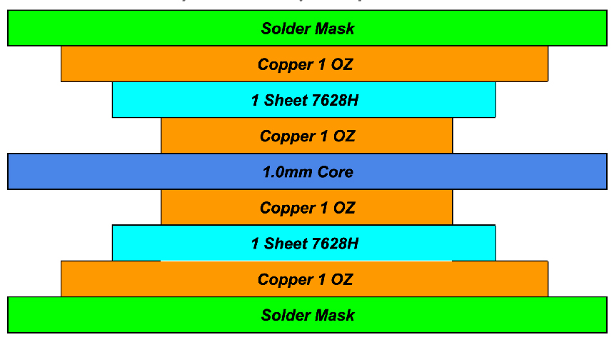
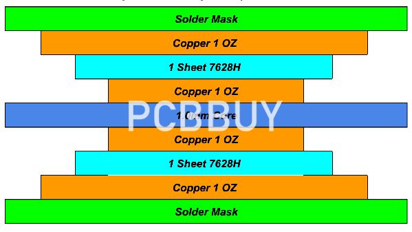
When you define a PCB stackup, you are establishing the precise arrangement of copper and insulating layers that form a printed circuit board (PCB). This configuration plays a critical role in signal integrity, electromagnetic compatibility (EMC), and the overall performance of modern electronics. Especially for high-speed or high-density applications, the PCB stackup design must be carefully planned to balance performance, manufacturability, and cost.
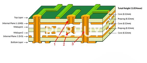
A PCB stackup is the vertical arrangement of conductive (usually copper) and dielectric (insulating) layers in a PCB. This stackup is defined before the layout process and dictates how power, ground, and signal layers are distributed across the board.
Why Defining a PCB Stackup Matters?
-
Improves electromagnetic compatibility (EMC).
-
Supports high-speed signal integrity.
-
Reduces crosstalk and radiation.
-
Enhances power delivery throughout the board.
-
Affects manufacturability and cost-efficiency.
✅ Pro Tip: Most advanced PCBs today use 4 to 16 layers, depending on complexity.
Standard PCB Stackup Thickness
Common PCB Thickness Standards
-
62 mils (1.57 mm) — Traditional standard.
-
93 mils (2.36 mm) and 125 mils (3.17 mm) — Increasingly common for multi-layer, high-performance PCBs.
Factors That Define PCB Stackup Thickness
|
Factor |
Description |
|
Copper Weight |
Heavier copper = thicker board |
|
Layer Count |
More layers = higher total thickness |
|
Dielectric Material |
Varies by Dk (dielectric constant) |
|
Environmental Tolerance |
High-temp or high-current environments require custom stackups |
When You Define a PCB Stackup Effectively?
1. Enhanced Signal Performance
Proper layer allocation ensures that signal traces have dedicated ground reference layers, which minimizes return path noise and electromagnetic interference.
2. Improved Electromagnetic Compatibility (EMC)
Isolating high-speed signal layers between ground planes reduces emissions and increases compliance with international EMC standards.
3. Noise and Crosstalk Mitigation
Strategic separation of noisy power circuits and sensitive analog/digital signals within the PCB stackup reduces signal degradation.
4. Better Thermal Management
Thermal vias and thick copper layers in power planes help dissipate heat efficiently, especially in high-power designs.
Modern PCB Stackup Configuration
Multilayer Design Trends
Modern PCBs are evolving from 2-layer boards to 4-, 6-, 8-, and up to 16-layer boards. The layer count is determined by:
-
Application complexity
-
Signal frequency
-
Pin density
-
Power/signal integrity requirements
📊 Statistical Insight: According to IPC standards, the global average for industrial-use PCBs is now 6 to 8 layers.
Common 4-Layer PCB Stackup Example
|
Layer |
Function |
|
Top Layer |
Signal |
|
Inner Layer 1 |
Ground |
|
Inner Layer 2 |
Power |
|
Bottom Layer |
Signal |
When You Define a PCB Stackup in Design?
Vertical vs. Horizontal Planning
A comprehensive PCB stackup design requires three-dimensional thinking, including:
-
Vertical Planning:
-
Dielectric thickness
-
Via types (through-hole, blind, buried)
-
Copper weights and plating
-
Horizontal Planning:
-
Trace width/spacing
-
Pad-to-pad clearance
-
Power and signal trace isolation
Critical Parameters for Defining a PCB Stackup
|
Parameter |
Importance |
|
Dielectric Constant (Dk) |
Affects impedance control |
|
Coefficient of Thermal Expansion (CTE) |
Critical for thermal reliability |
|
Copper Thickness |
Impacts current-carrying capability |
|
Via Design |
Influences signal routing and solderability |
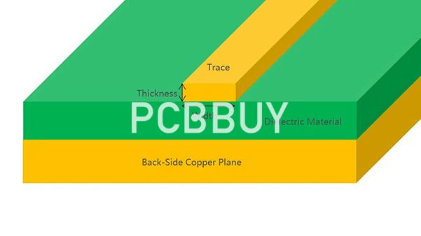
Define a PCB Stackup in Collaboration With Manufacturer
Always consult your contract manufacturer (CM) early in the design process to ensure your defined stackup is manufacturable and cost-effective. Their fabrication constraints and DFM (Design for Manufacturing) guidelines should influence:
-
Layer count limits
-
Minimum trace widths and spacing
-
Drill hole tolerances
-
Stackup symmetry requirements
Manufacturing Tip: PCB fabs often have predefined stackup templates—ask for their impedance-controlled stackup library for faster prototyping.
Conclusion
To define a PCB stackup is not merely a mechanical task—it is a critical engineering decision. The correct layer arrangement determines whether your design will meet signal performance targets, EMI requirements, and thermal limits. A properly defined PCB stackup is the backbone of high-reliability electronics in industries like aerospace, automotive, medical, and high-speed computing.
Industry Category


