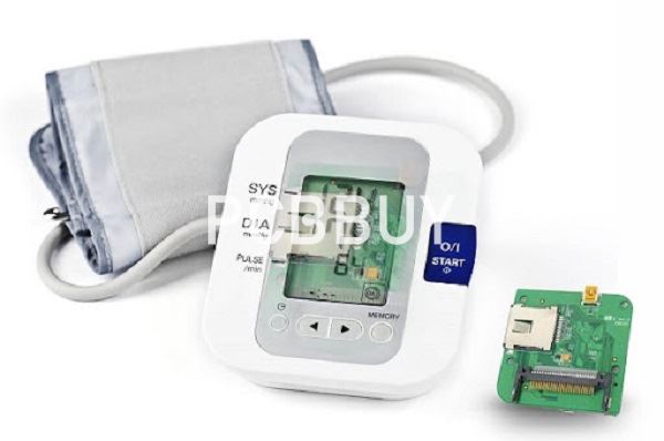
How to Design A Medical Device in PCB Manufacturing?
By:PCBBUY 03/14/2022 10:54

To ensure successful product launch, we offer design and engineering assistance to our medical device customers. This is particularly important because not only must we deliver the prototypes quickly, but they must be manufacturable in volume using the same processes that were used to manufacture the prototype.
Do you know the details of medical device in PCB manufacturing? In this passage, if you are going to learn more about medical device in PCB, please check and read the content below for more information.
How to design for medical device PCB?
You’re placing components and meticulously routing, routing, and re-routing. After that, you’re re-routing some more. While you’re paying attention to a myriad of minutia, it’s easy to forget the things that are most obvious to the people who will actually be assembling, taking apart, and re-assembling your device (even though it’s entirely likely that you’ll be one of them). Are your connectors arranged so that a human hand can reach into the assembly and mate them to their cables? Do pads connected to ground fills have thermal relief connections to ease solderability? Have you exported a 3D model of your board to do a virtual test fit in the assembly? Where are your components placed?
My biggest serviceability nightmare was when I made the mistake of using screw terminal blocks for several connectors. This saved time in initial assembly (no crimping!), but meant that every time the board was removed for debugging, every terminal had to be unscrewed. Every time this happened, I wished I’d just crimped together some cables and used Molex connectors (or anything other than terminal blocks).
What are the considerations of medical device PCB design?
Design with modifications in mind. For a first board spin, you’re kidding yourself if you think that everything is going to work the first time. I know a senior engineer who says that he’s done this once. My first rule of thumb is to make sure that all traces are accessible from the top layer. This makes them easy to cut, scrape away solder mask, and solder to. The second is make vias and test points large enough that you can easily solder jumpers to them if you need to. While modifying boards, components that are placed too closely together can make modifications difficult. Putting extra space between components can help with this, so when you’re doing your layout, feel free to use up the entire board.
Design your board so that it’s easy to test and debug. On the subject of things not working the first time, add test points. Lots of test points. Put them on your signal traces, put them on the output of your power supplies. Put them everywhere. Many times I’ve found myself wishing there was a test point on a particular trace. I’ve never found myself wishing that there wasn’t one. Also, if you keep the test points (and as many components as possible) on the side of the board that is exposed while the board is installed in the assembly, testing will be much easier.

Recycle your old circuit. Is there a sub-circuit from a previous design that perfectly suits the needs of your current project? Consider saving time by re-using a sub-circuit from a previous design. Switching power supplies are a good example of circuits that are often easily transferable from one design to the next. It can be tempting to design everything from scratch, but it’s often best to avoid doing things twice if you don’t have to.
Put down the footprint(s) for the component(s) that you aren’t sure you need just in case. Is there a component or sub-circuit that you think you might need, but you’re not sure? For instance if you think that maybe an RC low-pass filter at a certain analog input is a good idea, but you don’t know if it’s necessary, you can easily leave out the low-pass filter and put a zero-ohm resistor in place of an actual resistor to avoid having an open circuit.
Most of the time, more copper is better. I generally put a ground plane on all layers. Stitch your ground planes together with lots of vias. If you have both analog and digital sub-circuits on your board, it’s best to split the ground planes to minimize the noise that the digital circuits will impart onto analog circuits.
What are the common problems of medical device PCB design?
Schedules
Not only has the growth in the medical equipment industry escalated with more new devices available than ever before, but the competition within the industry has increased in intensity. Medical innovators need contract manufacturers that have a history of being able to hit the ground running with rapid prototyping that gets their products ready for the market imminently. This means that PCB CMs need to be prepared with design engineering, component procurement, and manufacturing teams that understand the critical nature of these schedules, and can respond quickly.

Production
While the goal of PCB manufacturing is to assemble circuit boards at the highest level of quality possible, this level of precision is much more critical in the production of medical equipment. These devices must be robust enough to work flawlessly in many different environments and conditions. Achieving quality like this requires more than just good soldering skills. It also includes precision in every aspect of manufacturing such as engineering, component procurement, assembly preparation, inspection, rework, and test.
Certification
It is also important that PCB CMs carry the certifications required to build medical equipment. Some of these include general certifications such as ISO 9001 for quality and reliability in manufacturing, or IPC-A-610 for the acceptability of printed circuit board assemblies. There are also specific certifications such as ISO 13485 which specifies the quality management system standard of devices built for the medical industry.
Industry Category


