How to Design PCB Antenna of NFC ?
By:PCBBUY 04/29/2022 13:55

When the dynamic NFC tag chip operates in RF mode, it is powered by the reader. No
battery is required to access it in RF mode, neither in read nor in write mode. The dynamic
NFC tag chip draws all the power it needs to operate from the magnetic field generated by
the reader through its loop antenna
Are you going to learn more about NFC PCB antenna design? If you are searching for the professional knowledge of NFC PCB antenna design, please check and read the content below in this passage.
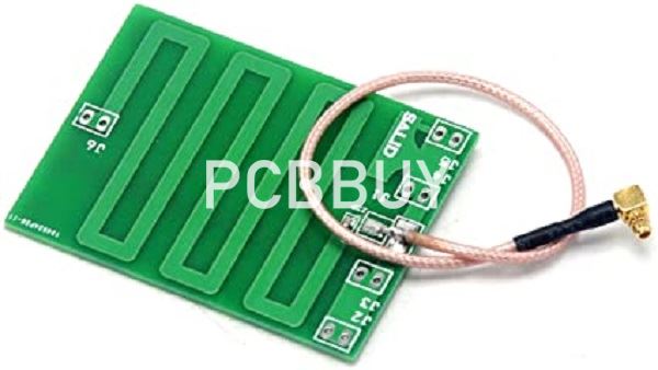
What is the quality of NFC PCB?
The selection of the correct NFC PCB manufacturer is a significant concern. The term quality may signify a range of various things and is not specified and may be vague in itself.
However, in essence, the NFC PCB quality implies that the panel comes in and draws – no mistakes.
· The quality of PCBs might indicate a multitude of aspects:
· Board in the proper size
· All hole drilled and placed precisely
· Test bare board passes
· Minimum bending of the board (although some of this can be due to board design)
· A lot of additional problems.
The performance should always remain excellent and not decline once the primary orders have been acquired successfully.
What is the working principle of NFC PCB?
The initiator (emitter) actively produces an RF field via magnetic fields between parallel circuit NFC antennas that may provide a passive goal (Tag).
Emitter antennas and the tag are connected via electrostatic energy, and best this system can be seen as an air-core converter, where the reader acts as a primary winding and the tag as a secondary winding: the alternative charging current through the superior (Emitter) induces an airfield that induces currents into the secondary belt (Tag). The tag may utilize the field current to power itself. In this instance, no battery is needed in reading or write mode to access it. The NFC tag chip gets all power required to function from the viewer’s produced magnetic field via its receiver coil.

What is inductance NFC PCB Antenna?
An NFC tag must have a PCB NFC antenna to connect and be powered. The antenna design process begins with the NFC chip approximate solution and its loop antenna:
· VOC is the open-circuit voltage of the loop antenna caused by a magnetic field
· Ra is the corresponding loop antenna resistance
· La is the comparable loop antenna inductance
· Rs is the NFC chip’s serial equivalent resistance
· Cs is the conventional equivalent NFC chip tuning capability
An inductance La with a very modest loss resistors Ra may define the antenna. When the transmitter in the loop antenna induces a magnetic field, there is a current there, and an open-circuit voltage Voc emerges at its terminals. The resistive input Rs and a built-in tuning condenser Cs may define the NFC PCB chip.
What are the applications of NFC PCB?
NFC is an emerging technology that needs to link electrical devices wirelessly. To communicate with hardware devices suitable with NFC and enable new services, such as contactless payment, NFC has been increasingly implemented into devices.
Because NFC tags do not require a power source to be included since they may be driven by the energy the reader emits, it may take extremely basic operating systems such as electric powered tags, NFC stickers, NFC card manufacturers, and even rings.
What is the importance of PCB NFC antenna?
An NFC tag must have a PCB NFC antenna to connect and be powered. The antenna design process begins with the NFC chip approximate solution and its loop antenna:
VOC is the open-circuit voltage of the loop antenna caused by a magnetic field
Ra is the corresponding loop antenna resistance
La is the comparable loop antenna inductance
Rs is the NFC chip’s serial equivalent resistance
Cs is the conventional equivalent NFC chip tuning capability
An inductance La with a very modest loss resistors Ra may define the antenna. When the transmitter in the loop antenna induces a magnetic field, there is a current there, and an open-circuit voltage Voc emerges at its terminals. The resistive input Rs and a built-in tuning condenser Cs may define the NFC PCB chip.

For the final approximate solution of the network containing the NFC integrated circuit and its integrated circuit, the resistors Ra and R are added together.
The NFC IC resistor Rs and the resistive antenna Ra and the built-in condenser Cs create a resonant RLC circuit with antenna inductor La.
The formula shows the frequency response of an RLC series:
F is the frequency of resonance (Hz)
L is the circuit inductance equivalent (H)
C is the equivalent circuit capacitance (F)
Industry Category


