How to Design RF PCB with 7 Most Reliable Tips?
By:PCBBUY 10/25/2021 10:48

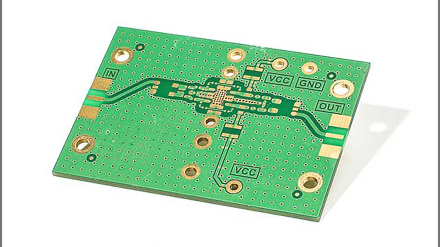
RF PCBs are one of the fastest growing sectors in PCB manufacturing. With with proliferation of IoT sensors, wireless electronics, and smart phones, it’s easy to see why. But how do you know if you’re working on an RF PCB? The PCB industry considers any board that operates above 100MHz to be an RF PCB. Anything about 2GHz is a Microwave PCB.
Are going to learn more about RF PCB design? If you are interested in RF PCB design, you can choose to check and read the content below for more information.

1. How to transmit line layers of RF PCB?
Does your RF layout require you to move a transmission line between layers? Maxim recommends using at least two via holes for each transition point to minimize via inductance loading. The width of these transition vias will need to match the width of the transmission lines. Used effectively, these vias can help to cut transition inductance by 50%.
2. How to select right material for RF PCB?
Materials commonly used in PCB fabrication, such as FR-4 (flame retardant level 4), are very cheap but are generally not the most suitable choice for high frequency RF applications, especially considering the non-uniformity of the dielectric constant and a worse tangent angle. For RF PCBs, specific materials are used, such as FEP, PTFE, ceramic, hydrocarbons, and various types of glass fiber. The PFE and PTFE materials, belonging to the fluoropolymer family, improve the chemical resistance of the base material, have anti-adhesion and smoothness properties, as well as an extraordinary heat resistance. If budget is not a problem and quality is more important than price, the best solution is PTFE with fiberglass, eventually woven glass fiber.
3. How to process the isolation of RF PCB?
Particular attention must be paid to avoid dangerous couplings between the signals. The RF transmission lines should be kept as separate as possible from other traces (especially if crossed by high-speed signals such as HDMI, Ethernet, USB, clock, differential signals, etc.) and not travel long stretches parallel to each other. The coupling between parallel microstrips, in fact, increases as the distance that separates them decreases and the distance traveled in the parallel direction increases. Similarly, traces carrying high-power signals should also be isolated from other parts of the circuit. An excellent insulation value can be obtained by using the grounded coplanar waveguides.
Traces carrying high-speed signals should be routed on a different layer than RF signals, in order to avoid coupling phenomena. The power supply lines should also be routed on dedicated layers, by inserting suitable decoupling/bypass capacitors.

4. How to process routing for RF PCB?
The ground wire should be as thick as possible. If it is possible, each layer of the PCB should be grounded as much as possible, and the ground should be connected to the main ground. More ground vias should be made to reduce the ground impedance as much as possible.
The power supply of the RF circuit should not be divided into planes as much as possible. The entire power plane not only increases the radiation of the power plane to the RF signal, but also is easily interfered by the RF signal. Therefore, the power cord or plane generally adopts a long strip shape and is processed according to the size of the current. It is as thick as possible under the premise of meeting the current capacity, but it cannot be widened without limit. When handling power lines, be sure to avoid loops.
The direction of the power line and the ground line must be parallel to the direction of the RF signal but not overlap. It is best to use a vertical cross where there is a cross.
5. How to process the component placement for RF PCB?
When placing components on an RF circuit board, the needs of the circuitry often demand a tighter part placement. Modifying the component placement is one of those compromises that the designer must carefully manage to ensure that the board can still be built with standard automated assembly equipment to keep production costs from escalating. RF boards also tend to have more metal on the external layers for their power networks, and components are often placed directly on those areas. While this connection may be better for the performance of the RF circuitry, it can cause problems for PCB assembly.
Another aspect of RF PCBs to keep in mind is that the components may require altering during layout. These can range from changing the size and shape of the PCB footprint pads to incorporating specific metal features and shapes into the footprint. Work like this is usually done individually to components on the board instead of altering the base library part. Next, we’ll list some of the routing requirements you may encounter on an RF PCB design.

6. What are the regular rules for RF PCB design?
These will include:
Design for Manufacturing (DFM) rules. If your design can’t be built because of basic DFM rules violations, you’ve got a much bigger problem on your hand. This includes designing your board for both assembly and test (DFA & DFT).
Keep in mind the basic PCB design rules for digital, analog, power, and mixed signal technologies. Just because you need more room for high speed traces or RF shielding doesn’t mean that you can ignore your regular PCB design spacing rules and squeeze things together.
Thermal issues with components run hot. High speed circuitry tends to generate more heat, and you need to keep thermal issues in mind now more than ever. Make sure that you board is getting cooled the way that it should be.
7. How to process high-speed RF PCB?
For success in routing high speed and RF circuitry on your PCB design, you need to follow some basic guidelines that will help you to avoid the more common problems. One of the first is to make sure that your schematic is set up with enough information to help the designers in layout with their routing. Another is to know precisely what materials and stackup configuration your high speed or RF design needs so that critical design data such as trace widths and spacing don’t change in mid-layout. Component placement also needs to be precise in order to produce short and direct signal paths, while high speed trace routing needs to follow topology patterns designed to create the best signal integrity performance.
Industry Category


