How to Determine Creepage Distance on PCBs?
By:OCBBUY 04/28/2025 15:00

Creepage distance is a critical parameter in PCB design, especially in applications where high voltages are present. It determines the shortest path along the surface of an insulating material between two conductive parts. Proper calculation of creepage distance ensures electrical safety and reliability by preventing electrical arcing and leakage currents. This article provides an in-depth guide on calculating creepage distance in PCBs, discussing its importance, influencing factors, standards, and practical considerations.
What is Creepage Distance?
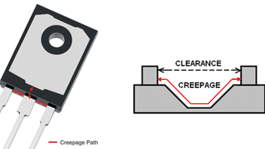
Creepage distance refers to the shortest path between two conductive elements measured along the surface of an insulating material, such as the PCB substrate. Unlike clearance, which is the direct air gap between conductors, creepage considers the surface path, which can be influenced by factors like surface contamination, humidity, and material properties.

What Is Importance of Creepage Distance in PCB Design?
Ensuring adequate creepage distance is crucial for:
Electrical Safety: Prevents unintended electrical discharges that could lead to short circuits, fire hazards, or electric shock.
Component Reliability: Reduces the risk of dielectric breakdown, ensuring long-term performance and stability of electronic components.
Compliance with Standards: Adherence to industry standards and regulations, such as IEC, UL, and IPC, which specify minimum creepage distances based on operating voltages and environmental conditions.
What Are the Factors Influencing Creepage Distance?
Operating Voltage
Higher operating voltages require greater creepage distances to prevent electrical arcing. The relationship between voltage and required creepage distance is not linear; it depends on the breakdown voltage of the insulating material and the environmental conditions.
|
Voltage Range |
Minimum Creepage Distance (mm) |
|
0 - 150V |
1.0 |
|
150 - 300V |
2.5 |
|
300 - 600V |
5.0 |
|
600 - 1000V |
8.0 |
Environmental Conditions
Pollution Degree: Describes the expected level of contamination in the operating environment, affecting the surface conductivity of the insulating material. Standards often classify environments from Pollution Degree 1 (clean room) to Pollution Degree 4 (severe industrial environments).

Humidity: High humidity can lead to condensation on PCB surfaces, increasing the risk of creepage-related failures. Designers must consider the relative humidity of the environment when calculating creepage distances.
|
Pollution Degree |
Description |
Typical Environments |
|
1 |
No pollution or only dry, non-conductive pollution |
Clean rooms, controlled environments |
|
2 |
Non-conductive pollution that can become conductive |
Office buildings, laboratories |
|
3 |
Conductive pollution expected |
Industrial areas, manufacturing plants |
|
4 |
Persistent conductive pollution |
Outdoor installations, severe environments |
Material Properties
The choice of PCB substrate material influences the creepage distance due to variations in dielectric strength and resistance to surface tracking. Common PCB materials include FR4, polyimide, and ceramic, each offering different levels of insulation and mechanical properties.
|
Material |
CTI (Comparative Tracking Index) |
Dielectric Strength (kV/mm) |
|
FR4 |
175 - 220 |
20 - 30 |
|
Polyimide |
150 - 250 |
30 - 50 |
|
Ceramic |
>600 |
15 - 40 |
PCB Design and Layout Considerations
Trace Routing: The layout of traces on the PCB can affect the effective creepage distance. Avoiding sharp corners and keeping high-voltage traces away from low-voltage areas can minimize creepage risk.
Component Placement: Proper placement of components, especially those with high-voltage differentials, is crucial. Insulating barriers or conformal coatings can also be used to increase creepage distance.

Standards and Regulations
International Standards
IEC 60664: Provides guidelines for insulation coordination for equipment within low-voltage systems. It specifies creepage distances based on working voltage, material group, and pollution degree.
UL 60950-1: Focuses on the safety of information technology equipment, including electrical business equipment. It outlines requirements for creepage distances to prevent electric shock and fire hazards.
Industry-Specific Standards
IPC-2221: The generic standard for PCB design, including guidelines for determining creepage and clearance distances. It offers tables and formulas for calculating these distances based on voltage, material properties, and environmental factors.
-MIL-STD-275: Used in military applications, this standard provides additional guidelines for PCBs used in harsh environments, where increased creepage distances may be required due to extreme conditions.
What Are the Calculation Methods for Creepage Distance?
Basic Formula
The basic formula for creepage distance is:
Dcreepage = k X V
where:
· Dcreepage is the creepage distance in millimeters,
· k is a constant derived from the material properties, pollution degree, and environmental conditions,
· V is the working voltage in volts.
Use of Standards Tables
Standards such as IEC 60664 provide tables that list minimum creepage distances based on various factors. These tables simplify the calculation process by providing pre-determined distances for specific conditions.

Example Calculation
Consider a PCB operating at 300V in an industrial environment (Pollution Degree 3) using FR4 material. According to IEC 60664, the minimum creepage distance for this setup might be determined as follows:
1. Determine the Material Group and Pollution Degree: FR4 typically falls under Material Group IIIa with a CTI of 175-220.
2. Check the Voltage Range: 300V falls under the range where a creepage distance of 5.0mm is generally required for Pollution Degree 3.
Thus, the PCB should have a minimum creepage distance of 5.0mm to ensure safety and compliance.
What Are the Factors of Safety?
To account for manufacturing tolerances, environmental variations, and potential degradation over time, a factor of safety is often applied to the calculated creepage distance. This ensures additional margin for reliability.
What Are the Practical Considerations in Creepage Design?
Conformal Coating and Potting
Applying conformal coatings or potting compounds can significantly increase the creepage distance by covering the PCB surface and reducing the risk of surface tracking. These coatings are particularly useful in harsh environments or where high reliability is required.
|
Coating Type |
Benefits |
Application |
|
Acrylic |
Good moisture resistance, easy to apply |
General electronics, low-cost applications |
|
Silicone |
High thermal stability, flexible |
Automotive, aerospace |
|
Silicone |
Excellent chemical resistance, durable |
Industrial electronics |
Component Selection and Placement
Careful selection and placement of components, particularly high-voltage components, can optimize the use of available space and ensure adequate creepage distance. For instance, components with higher isolation ratings can be used in critical areas to enhance safety.
Trace Separation and Routing
Increasing the separation between high-voltage and low-voltage traces can reduce the risk of creepage. Additionally, using routed slots or barriers between traces can effectively increase the creepage distance without altering the PCB layout significantly.
Environmental Sealing
In environments with high humidity or contamination, sealing the PCB in a protective enclosure can prevent the ingress of moisture and pollutants, thereby maintaining the effectiveness of the designed creepage distances.

Case Studies and Real-World Applications
Case Study 1: Industrial Power Supply
In an industrial power supply design, where components are exposed to high voltages and significant contamination, the use of increased creepage distances and conformal coatings was critical. By applying a conformal coating and maintaining a creepage distance of 8.0mm, the design met stringent safety standards and ensured reliable operation.
Case Study 2: Consumer Electronics
In a consumer electronics device, the miniaturization of components posed a challenge for maintaining adequate creepage distances. By utilizing high dielectric strength materials and innovative PCB layout techniques, the design team was able to achieve compliance with safety standards without compromising on the device's compact form factor.
Case Study 3: Automotive Electronics
An automotive control module required robust design considerations for creepage distance due to exposure to harsh environments and high voltages. By implementing a combination of conformal coatings, careful component placement, and increased trace separation, the module achieved high reliability and safety, even under extreme conditions.
Conclusion
Calculating and maintaining adequate creepage distances in PCB design is essential for ensuring electrical safety, reliability, and compliance with industry standards. By understanding the factors that influence creepage, such as operating voltage, environmental conditions, and material properties, designers can implement effective strategies to mitigate risks. Practical considerations, including the use of conformal coatings, careful component placement, and proper trace routing, further enhance the reliability of PCB designs in various applications.
References
1. IEC 60664-1: "Insulation Coordination for Equipment within Low-Voltage Systems," International Electrotechnical Commission.
2. UL 60950-1: "Information Technology Equipment - Safety - Part 1: General Requirements," Underwriters Laboratories.
3. IPC-2221: "Generic Standard on Printed Board Design," IPC.
4. MIL-STD-275: "Military Standard for Printed Wiring for Electronic Equipment," Department of Defense.
5. H. W. Johnson, M. Graham, "High-Speed Digital Design: A Handbook of Black Magic," Prentice Hall, 1993.
Industry Category


