PCB Via Size Guidelines: How to Determine Via Size with 5 Common Problems?
By:PCBBUY 09/22/2021 17:36

The trends toward smaller circuit boards--and electronics products in general--over recent decades is undeniable. However, the most important reason that the demand for smaller boards is able to be met is the increase in the use of multiple-layer stackups and vias. Vias come in various sizes and have different applications on circuit boards.
In this passage, we will provide you the PCB via size guidelines. If you are curious about how to determine the via size and what are the common problems during the process, please check and read the content for more information about it.
What are the considerations before determining PCB via size?
As with other choices for your circuit board design, your choice of via type and size should not be made without considering the impact on other aspects of your design and development process. For example, manufacturability should always be a major concern, as even the greatest design is useless unless it can be built.
Classification
Prior to selecting a via size, the board classification needs to be determined.
Fabricator equipment capabilities
Although most manufacturers have a robust range of drill hole sizes that they can produce, it is critical that you work with a CM that has the capability to produce the size vias that your design requires.
Board density
In addition to affecting your board’s classification, the density of components and other elements directly impact the clearance requirements and, consequently, the size of your stackup and the number of vias needed to meet operational objectives. Inadequate clearances and ill-designed stackups can significantly increase the EMI on your board, which degrades signal integrity.
Via density
Many boards, especially if comprised of high pin count SMT ICs, can have significant numbers of vias. Coupled with high-power requirements and the need for thermal vias, this can lead to high via density.

What are the 5 common problems during determining PCB via size?
Some via size considerations to remember when setting up the vias in your PCB design include:
1. Smaller vias
These vias are important in the support of smaller-pitch/higher-density components, such as 0.5mm BGAs, but they are more sensitive to drill and plating errors, which can cause PCB failures. Only use these smaller sizes when necessary. It is much better for manufacturing to use an 8 mil hole instead of a 5 mil hole if it will only take minor layout modifications to do so.
2. Larger vias
These are much easier for the fabricator to work with, but the correct tolerances and clearances must be used to ensure there aren’t any shorts to other layers. It is also important to consider where the placement of larger vias will be so that they don’t pull the solder away from ground pads that need a good connection to their component.
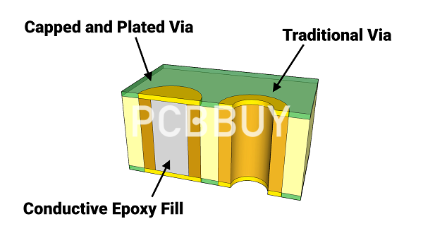
3. Blind and buried vias
These are essential for high-density, high-speed, noise-sensitive designs, but their advantage comes with a price. These vias require increased fabrication costs and time to process the vias first before laminating the layers of the board together.
4. Too many vias of the same size
Try to vary the drill sizes so that you don’t have too many holes that are the same size. For those boards with a high density of the same drill size, the drill bit may not be able to keep its integrity for the entire drill operation. This requires the fabricator to stop the drilling process partway through, replace the drill bit, re-register the board, and then continue the operation.
5. Plating
Your holes will be plated with copper for connectivity unless you specify the hole as being unplated. Make sure that you specify the correct size for the drill needed for the hole taking into account the plating. Usually, this is done by specifying the “finished” hole size. If the finished (plated) hole size isn’t accounted for, you may end up not being able to insert the component leads into their holes.

What are the specialize demands for PCB via size?
If you want to access the inner layers in a multi-layer PCB, you’ll need to use vias to route your signal, power, and ground lines. The best via size depends on a number of factors. Most important is your trace width, which is related to trace density, especially in an HDI board.
If you’re working with a board that uses a lower trace density, fewer components, and a smaller number of layers, you can usually get away with using plated through-hole vias with a relatively large diameter. Your traces can handle higher current and will have lower IR losses.
Once you need to accommodate more traces on your board and when you have a large number of components, real estate becomes a precious commodity. You’ll need to use thinner traces in order to save board space. In a multi-layer board, you’ll need to use smaller vias to access the inner layers, which increases the aspect ratio of your vias.
When you need to determine the best via size to use in a multi-layer PCB, you’ll need to have an idea of the thermal demands that your via can withstand. This is a function of the electrical power dissipated in the trace, any appreciable IR losses, and the geometry of your traces and vias. Any heat generated by nearby components can also dissipate into vias and increase their temperature.
Industry Category


