How to Find PCB Footprint Step by Step for Beginners?
By:PCBBUY 01/21/2022 09:09

There are several ways to create your PCB footprint library, and the first is to use existing library parts. In many cases, the vendor or supplier of the PCB design tools you are using will already have vast libraries from which you can pull parts. There are also many component vendors out there who will offer a footprint of the specific part you are using tailored for the design tools that you are working on. The advantage here is that, since these footprints are created by the component vendor, they are usually very accurate.
In this passage, we will provide all the information about PCB footprint. If you are searching for the knowledge of PCB footprint, check and read the content below for more.
What are the issues of PCB footprint?
Today, the industry is more aware of the need to follow PCB footprint creation guidelines because wasted space isn’t the only thing that can happen if a footprint is created incorrectly. Here are some of the other problems that you might see:
Incorrect pad sizes: Pads that are too small can cause breakout problems for through-hole parts and bad solder joints for surface mount technology (SMT) parts. Pads that are too large can take up room for trace routing or cause SMT parts to float out of position during soldering.
Pads that are not spaced correctly: Through-hole pads that are too close together or too far apart can cause problems with component insertion during assembly. SMT pads that are too close or too far from each other can cause insufficient solder joints to be formed, as not enough of the component lead is available for soldering.
Component outlines that are too small: Footprints that have their body outlines drawn too small will not be able to be assembled using automated production lines. Depending on the severity of the error, the parts may be able to be manually assembled, but that could take extra time and expense. For large errors, the boards may be completely rejected by the manufacturer. As you can see, it is very important to get the size of the PCB footprint correct before it is used in the design. Having to redesign a circuit board because of a footprint error can prove costly from a time and money perspective. Here are some footprint creation recommendations, however, that can help.

What are the basic guidelines of PCB footprint design?
Your PCB component footprints should include several basic pieces of information. Things like placement, assembly, and silkscreen outlines, reference designators and part numbers are all invaluable and should be present in a component footprint. Your CAD tools are invaluable here as you can create your 2D footprints in a variety of file formats. However, it is best to use the CAD tools in your PCB design software to ensure file compatibility. There are four important points to remember when creating PCB footprints:
I remember creating my first PCB footprint from a datasheet. A thorough datasheet will show a drawing of the component with all dimensions, pad locations, pad sizes, and any other important features that should be included in a PCB footprint. Some components, such as power MOSFETs, may contain an integrated heat sink or die-attached paddle that needs to be included in the component footprint. This is quite important for high voltage designs and high speed designs as these elements are included in some thermal and electrical simulations.
Whether you can find a library for your part, have one built for you or must create one yourself, you need to ensure that the footprint pad layout adheres to the following guidelines:
· Make sure that the component pad layout is symmetric. This will prevent tombstoning, which is the detachment of one side of the component due to unbalanced stress.
· Make sure that opposite pads for a single component have the same size and shape. This helps prevent tombstoning and component shifting.
· Make sure that the solder mask dam between footprint pads and all other surface elements (i.e. other component footprint pads, traces and drill holes) is adequate. This prevents solder bridging, which occurs when solder joints intended to be separate are too close together. It also allows for the application of solder mask, which protects the board from the environment.
· Make sure that clearance between footprint pads and the board edge is sufficient. This helps with depanelization, which is the separation of the processed panel into individual boards.

How to process PCB footprint design?
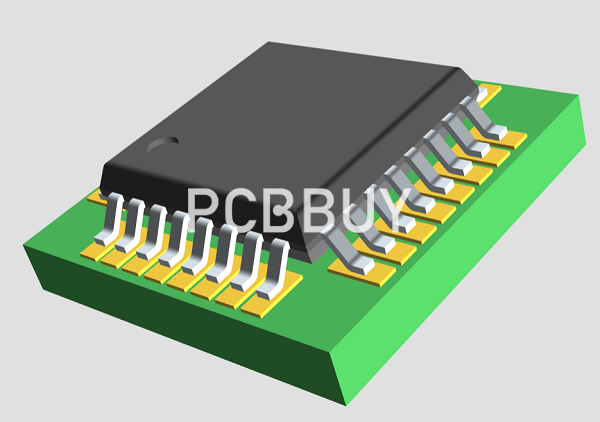
A footprint is the physical layout of the sizes, shapes, and separation of the pads that need to be placed with exposed copper on the bare board so that a component placed on top can be soldered down accurately, with the right pins connecting to the right electrical nets. PCB design packages allow you to draw the schematic of the circuit symbolically and to link each component to an appropriate footprint so that when the designer moves to the board layout phase all of the wires will be connected to each component as specified by the schematic.
Footprint of a compliment marks the area occupied by itself on board along with indication of points of connection ( for soldering ) Footprint of components are used for designing of a PCB. These footprints are moved at appropriate location on the board before routing ( drawing path for electrical connection ). Footprint helps in determining spacing between components and also helps in routing. Spacing between components is important factor from production point of view, as well as design point of view.
Industry Category


