How to Fix Broken PCB Traces with 7 Necessary Methods?
By:PCBBUY 10/15/2021 09:27

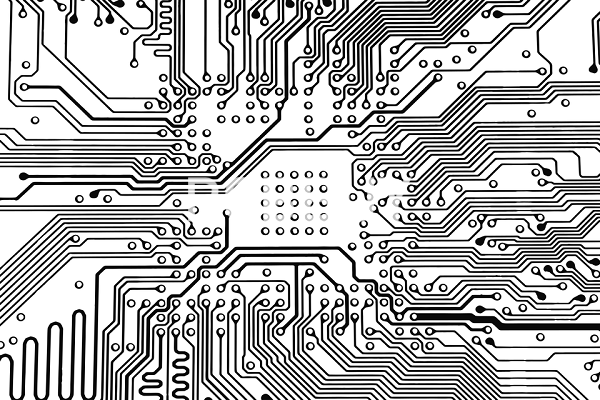
Printed Circuit Boards (PCB) are made from layers of fibreglass and copper, glued together. Whilst the glues used are very heat resistant it is possible to overheat a PCB and damage it. Kitronik PCB designs use large tracks and pads to help make this a rare problem, the larger amount of copper helps to dissipate the heat.
If you are interested in the methods of fixing broken PCB trace, in this passage you could learn more knowledge of fixing broken PCB trace. You can check and read the content below for more information.
1. How to identify the broken PCB trace?
The traces on a printed circuit board are pathways that conduct electricity and consist of either copper or silver. PCB trace damage that occurs as a result of physical breakdowns or ongoing use can lead to major problems that affect the parts and conductivity of the printed circuit board and the actual device.
There are different causes of trace damage and these include regular wear and tear, overheating, dust, power surges and lightning. If the trace is not hard to see due to being extremely thin, it is generally possible to identify the damage by examining the pathway.
Since silver and copper are naturally bright and conspicuous elements, they are easy to detect when there is a problem. Fixing damaged or defective pathways involves using the right material to solder the board in order to restore the damaged circuit and enable electricity to flow without disruption through the circuit board.
2. How to bridging broken PCB traces with wire?
You won’t be able to solder directly over the broken traces. There’s an epoxy coating over most of the metal that solder won’t adhere to. You can scrape away the epoxy with an awl or a pick until you get down to bare copper. You’ll know when you reach copper, as the color changes from the tint of the PCB to bright, shiny copper like a new penny. Expose a good 1/8 inch or 3 mm of the trace, if not a bit more. Clean the area, then apply a bit of flux to the bare copper.
Strip a bit of wire and tin the end, then solder the wire to one side of the trace. Cut the wire to length, then strip and tin the other end. Position the wire on the board and apply a bit of tape to hold the wire in place if you need to. Solder the other end, then remove the tape. Let the solder cool, then check to make sure the wire stays in place. You want bright, shiny solder joints, not dull ones. Dull joints indicate both a weak electrical and mechanical bond.

3. What is the process of fixing broken PCB traces?
· Mix the epoxy according to the manufacturer's instructions, and apply it sparingly to one side of the PCB. Press the two halves of the broken board together, and hold them until the epoxy takes hold.
· Cut through the broken copper traces using a razor knife. Remove all of the loose traces, and then carefully use the emery cloth to sand the traces from which you removed the loose sections.
· Plug the soldering pencil into a 110-volt receptacle and wait for it to get hot. Clean the hot soldering tip by wiping it on a wet soldering sponge.
· Apply a fresh "tinning" coat of rosin-core solder to the clean soldering pencil tip. A properly tinned tip will be a bright silvery color.
· Apply the rosin-core solder to the bared copper traces on the printed circuit board. Use care to apply no more heat than is necessary to melt the solder.
· Cut pieces of the 18-gauge copper wire that are long enough to span the cut traces, and tin these short lengths of wire with rosin-core solder.
· Pick up a piece of tinned wire with the tweezers and lay it carefully across one of the traces where you removed a loose section.
· Reassemble the device and test it to see if it works properly.
4. How to prepare the soldering for broken PCB traces?
Next, you will have to prepare the printed circuit board for soldering to reestablish the wired connection between the boards. For this, at first, find a 110V receptacle (power source) and plug in the soldering pencil in it.
Then wait until the soldering pencil becomes hot. When the soldering tip gets hot, wipe it using a wet soldering sponge. Make sure to plug off the soldering pencil before wiping it on the sponge. Also, ensure that the tip is free from every dirt and oxidation for fine soldering later.
5. How to layer the wiring of broken PCB traces?
Use tweezers to pick the tinned wires one after one carefully. Then lay the picked wiring right on the traces from where you have removed the loose traces lately.

After you have layered the copper wiring on the traced gaps, you will require soldering them properly. For this, use the soldering pencil tip and fuse the 18-gauge copper wiring accurately in the holes. You will have to repeat the wiring procedure to fill up each loose trace and link the wiring appropriately.
6. How to locate the broken PCB traces?
Use the free millimeter’s probe to touch a single spot on the board. Then use your finger with the foil move it over the components touching the soldered part. Thus you will cover more area quicker and when you hear the millimeter beeping - you have found your track on the PCB.
7. How to text he broken PCB traces?
The A stands for the amp which is the unit for electrical current. Test all devices on the circuit board, one at a time, by touching the red and black probes of the millimeter to either side of the device. A zero current reading indicates a short circuit.
Industry Category


