How to Fix PCB Annular Ring Breakout During Fabrication
By:PCBBUY 10/28/2026 15:55

Introduction
Annular ring breakout is a common PCB fabrication issue that occurs when a drilled hole extends beyond the copper pad intended to surround it. The result may be a partially or completely missing copper ring, potentially weakening the connection between a plated-through hole and its associated copper trace.
For automotive electronics, industrial control systems, power equipment, and energy-storage products, preventing annular ring breakout is important for manufacturing yield and electrical reliability. The most effective solution is to identify whether the problem originates from pad design, drill registration, layer alignment, or an incorrect interpretation of the acceptance criteria.

1. What Causes PCB Annular Ring Breakout?
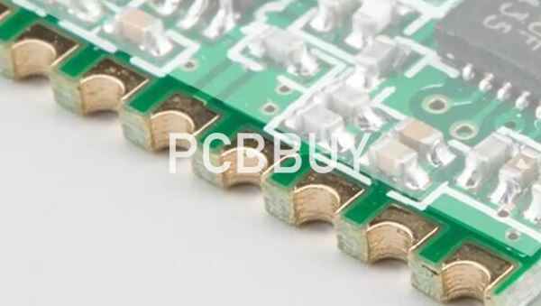
An annular ring is the copper surrounding a drilled hole on a PCB layer. Breakout occurs when the hole extends beyond the pad boundary, reducing or eliminating the copper connection on one side.
Common causes include:
-
Insufficient pad diameter: The copper pad does not provide enough margin for the specified hole size and manufacturing tolerances.
-
Drill-position deviation: The actual drill location differs from the intended pad center.
-
Layer registration error: Inner-layer artwork and drilled-hole positions are not aligned closely enough.
-
Incorrect hole-size assumptions: The design does not adequately account for the relationship between the drilled hole, finished hole, and copper plating.
-
Inadequate DFM review: Annular ring and drill-to-copper clearances are not checked against the manufacturer's actual process capability.
Breakout is not always equivalent to an electrical open circuit. Its acceptability depends on the affected layer, remaining copper connection, product class, applicable IPC requirements, and customer specification. However, a breakout that severs a required trace-to-pad connection can cause an open circuit and must be addressed.

2. How to Fix Annular Ring Breakout
Increase the Pad Diameter When Space Allows
The most direct design correction is to enlarge the pad while preserving the required clearance from neighboring copper features. A larger pad provides more tolerance for drill-position deviation and helps maintain a continuous copper ring after drilling.
The annular ring can be estimated from the pad and hole diameters:
Nominal annular ring width = (Pad diameter − Hole diameter) / 2
This is a nominal geometric calculation. Final acceptance must account for the applicable hole definition, plating, registration tolerance, and measurement method.
Add Teardrops at Critical Trace-to-Pad Connections
A teardrop gradually widens the copper where a trace connects to a pad or via. It can help preserve the trace-to-pad connection when drill offset reduces the available copper.
However, a teardrop is not a universal cure. It may improve the connection on the trace side but cannot restore an inadequate annular ring on the opposite side of the hole. The pad size and drill geometry must still meet the applicable design and manufacturing requirements.
Review Drill and Layer Registration
If breakout appears across many pads or is concentrated on particular layers, the manufacturer should investigate drill positioning, inner-layer registration, panel movement, and the relevant fabrication tolerances.
The correct corrective action depends on the defect pattern. Enlarging every pad may be unnecessary if the underlying cause is a process-control or data-alignment issue.
Confirm Hole Definitions and Acceptance Criteria
The fabrication drawing should clearly identify plated through-holes, non-plated holes, finished hole sizes, and the required product class or acceptance criteria. The design team and manufacturer should use the same definition of nominal and finished dimensions.
Do not apply one annular ring value to every PCB. Requirements depend on the applicable standard, layer type, product class, and manufacturing process.
3. Prevention Checklist for PCB Designers
|
Design or process issue |
Recommended action |
|
Pad diameter too small |
Increase the pad or revise the via structure after checking routing clearance. |
|
Narrow trace-to-pad junction |
Consider a teardrop where design rules and electrical requirements permit. |
|
Insufficient drill registration margin |
Confirm actual fabrication tolerances with the PCB manufacturer before finalizing the layout. |
|
Inner-layer breakout |
Review layer-to-drill registration and the affected layer's copper geometry. |
|
Incorrect hole-size definition |
Align the drill table, fabrication drawing, and finished-hole requirements. |
|
Dense routing limits pad enlargement |
Evaluate alternative via sizes, placement, layer transitions, or routing geometry. |
|
Unclear acceptance requirements |
Specify the applicable IPC class and customer-specific criteria before production. |
4. How PCBBUY and PCBBBUY Can Help
For projects in automotive electronics, industrial control, power and electrical systems, power supplies, energy storage, new energy, and embodied robotics, annular ring design should be reviewed before fabrication data is released.
PCBBBUY can help coordinate customer requirements with PCBBUY's engineering review. PCBBUY's general manufacturing capabilities include multilayer PCB fabrication, HDI processing, fine-line fabrication, and inspection methods such as AOI and electrical testing where applicable.
Its stated general capabilities include boards up to 26 layers and minimum line width down to 35 μm (1.4 mil). These figures provide context for its broader PCB manufacturing capability, but they do not independently establish a specific annular ring tolerance or guarantee zero breakout for every design.
For a board with tight via geometry, provide the following during engineering review:
-
Gerber or ODB++ fabrication data and the complete drill files.
-
Finished-hole sizes and plated/non-plated hole definitions.
-
Layer stack-up, copper requirements, and the applicable product class.
-
Minimum annular ring and drill-to-copper clearance requirements.
-
Any special reliability, inspection, or acceptance criteria.
Engineering review should confirm whether the proposed pad and hole geometry is manufacturable within the agreed process window. Where the design is too tight, the preferred solution may be a larger pad, revised via geometry, a teardrop, or a change to the routing arrangement.
5. Inspection and Shipment Acceptance
A reliable corrective-action process should identify the defect, determine its cause, implement a design or process correction, and verify the result against the agreed acceptance criteria.
AOI can inspect accessible copper patterns and other visible features, while electrical testing can identify certain opens and shorts. Neither method alone proves that every internal annular ring meets its dimensional requirement. When necessary, suitable cross-section analysis or other agreed verification methods can be used to examine internal-layer registration and remaining copper geometry.
Shipment acceptance should be based on the approved fabrication data, applicable IPC requirements, customer specifications, and agreed inspection records. For high-reliability applications, the acceptance plan should clearly state whether breakout is permitted, what minimum ring is required, and how compliance will be verified.

Conclusion
Fixing PCB annular ring breakout requires more than simply increasing pad size. Designers and manufacturers must consider hole dimensions, pad geometry, drill registration, layer alignment, and the applicable acceptance criteria as one connected manufacturing problem.
By involving PCBBBUY and PCBBUY early, customers can identify high-risk via structures, resolve DFM issues before fabrication, and agree on practical inspection and shipment requirements for reliable PCB production.
FAQ
1. What is PCB annular ring breakout?
It occurs when a drilled hole extends beyond the copper pad boundary, reducing or removing part of the copper ring surrounding the hole. If the breakout severs a required connection, it can cause an electrical open.
2. What is the fastest way to prevent annular ring breakout?
First check whether the pad provides sufficient margin for the hole size and manufacturing tolerances. Enlarging the pad is often effective when space allows. Teardrops can help protect trace-to-pad connections, but they do not replace adequate annular ring design.
3. Can a PCB with annular ring breakout still be acceptable?
Potentially, depending on the affected layer, remaining connection, product class, applicable IPC requirements, and customer specification. The defect should be evaluated against the actual acceptance criteria rather than judged by appearance alone.
4. Does adding a teardrop eliminate all breakout risk?
No. A teardrop reinforces the copper connection between a trace and a pad or via, but it cannot compensate for every form of drill offset or inadequate pad geometry.
5. How can PCBBUY help prevent annular ring breakout?
PCBBUY can review the fabrication data, hole definitions, stack-up, and design constraints against the applicable manufacturing requirements. The specific annular ring capability and inspection plan should be confirmed with its engineering team before production.
6. Which inspection method can verify internal annular rings?
The appropriate method depends on the defect and acceptance requirement. Electrical testing can detect certain connectivity failures, while cross-section analysis can provide direct evidence of internal copper and drilled-hole geometry. The required method should be agreed before production.
Industry Category