How to Get to Know PCB Mouse Bite Dimensions for Beginners?
By:PCBBUY 12/03/2021 09:01

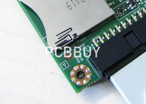
Mouse Bites are a line of tiny holes in a PCB board just like the holes around postage stamps, permitting small PCBs to be used in an array. The purpose of the mouse bites is for a better grip when mounted. Rat Bites can be economical for hand separating. While, thicker PCBs require more holes on the edge rails for easy break, and it is better with V-score for mechanical separation. The mouse bites, also called as perforated breakaway tabs, are the sharp edges, what are left over after depanelization when the PCBs are manufactured in a panel using break-routing / break-off tabs.
If you are a PCB beginner and you are going to learn the information about PCB mouse bite, please check and read the content below in this passage.
What is the basic definition of PCB mouse bite?
A mouse bite in a circuit board is part of the manufacturing panel used to fabricate and assemble the circuit board. Some people use the term “mouse bite” to describe over-etching in copper, but that isn’t what we are talking about here.
Circuit boards are typically laid out in a manufacturing panel by your PCB contract manufacturer using their Computer-Aided Manufacturing (CAM) systems. The panel gives both the fabricator and the assembler more board material for handling during the manufacturing processes, which is critical for smaller boards. Panels are usually a uniform size, and multiple instances of the PCB design can be laid out within the outline of the panel. Not only does a panel make it easier to manufacture a board, but multiple boards in the panel can be processed for almost the same cost as a single board.
Once the circuit boards have completed their fabrication and assembly processes, they need to be separated from their panels in a process called “depanelization.” Depanelization is accomplished by either cutting the boards out along pre-scored lines known as “V-grooves,” or breaking them out. Boards to be broken out must already be routed around their outlines to separate them from the panel and are only held in place by small tabs of material. These “breakout tabs” are removed, freeing the board from its manufacturing panel.
What are the main factors of PCB mouse bite?
The holes utilized for breakout tabs may vary. However, majority of manufacturers utilize five holes in breakout tabs having these dimensions.
The hole size is usually 0.5 mm or 0.020 inch in diameter. Concerning the spacing, they are 0.76 mm or 0.030 inches apart.
The spacing and sizes of the mouse bite PCB holes appear random. This reduces the cleanup needed after the breaking out of the board from the panel. Though, it takes less effort for a smaller hole to smoothen out, it will also need more holes to be drilled and leave out much bulk material.
However, if there are too big holes, the board will end up having mouse bites that are larger and will need smoothening out. The hole placement within this breakout tab is important as well. The goal here is drilling them nearer to the PCB edge. This helps in reducing the tab material leftover that needs to be removed.

Constraints to consider during placement of breakaway Tab PCBs
There are some constraints to consider while performing the breakout tabs’ placement around the outline of the board.
· Don’t make use of many tabs in order to save wear, effort, and time on its router bits.
· Have enough tabs that can support the PCB board fully in its panel throughout the operations of PCB assembly.
· Tabs having a minimum clearance of 0.125 inches should be located to the closest components.
· Don’t place the tabs close to circuitry or sensitive components areas. This could cause the board to experience more breakout stresses.
At times, stress damages coming to the circuitry or components due to the tabs breaking may not be seen till later. It may also cause intermittent issues that won’t be debugged easily. This is why the location of breakout tabs, a distance away from any sensitive area, is very important to the circuit board’s success.
Also, if you don’t use enough tabs, and you don’t place them strategically to support your board during the manufacturing process, your board may end up flexing too much. This will prevent a reliable assembly. Now, this is the point where the experience and knowledge of your PCB manufacturer comes in.
Industry Category


