How to Identify Multilayer PCB with 5 Essential Tips for Beginners?
By:PCBBUY 10/27/2021 09:30

These types of PCBs offer a range of benefits. One of the most common reasons for using the multilayer PCB is the size. Because of the layered design, it means that the PCB will be smaller than other printed circuit boards but still have the same level of functionality. Most people today want their electronics to be smaller, while still being powerful. The multilayer PCB allows for this. These types of boards also happen to weigh less, which helps to reduce the overall weight of the gadgets in which they are used. However, the size is certainly not the only benefit.
In this passage, we are going to provide you the methods to identify the multilayer PCB. If you are going to learn the professional knowledge, please check and read the content for more.
1. What are the advantages of multilayer PCB?
· Useful for more complex projects – Complex circuitry requires a multilayer PCB. Complex projects that need advanced equipment must-have tools with multilayer PCBs in them. Luckily enough, this is an easy thing for multilayer boards.
· High quality. – Unlike single and double-layered PCBs, multilayer boards require intense planning and production. Therefore, it means that they are of the highest quality compared to other boards.
· Increased power. – Based on increased circuit density that is characteristic of multilayer PCBs, this means that they are more powerful. Additionally, they run at very high speeds bringing about enhanced performance in equipment.
· Higher durability – Multilayer PCBs are highly durable, partly due to their stack up.
· Smaller in size and lighter in weight – More layers in a board mean thicker, hence durable. With more layers, such panels can effectively function in harsh conditions.
· Single connection point. – If you use several PCB components, you would need several connection points. But this isn't the case with multilayer PCBs. Their design is to work with a single point of contact. With such, the system becomes simple, and the weight also reduces.
2. What are the types of multilayer PCB?
Single-layer PCBs – It is one in which copper layer [thin] coating is on only one side of the board. On the other hand are connections of electrical components connected electrically.
Double layer PCBs – In this type of PCB, a thin layer of copper coating is on either side of the board. Drilled holes connect circuits of both parties.
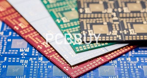
Multi-layered PCBs – It is a series of 3 or more double-layered PCBs. Insulation is between each PCB. They are in place through powerful glue.
Rigid PCBs – These PCBs use rigid substrate, which does not twist. It comes in a single layer, double layer as well as multi-layer PCB.
Flexible PCBs – These PCBs use flexible substrate material. It also comes in a single layer, double layer as well as multi-layer PCB.

3. What are the condiferations of multilayer PCB?
When considering how to determine PCB layers stackup, the best practices is to prioritize signal integrity. Signal integrity occurs when RF current generation is avoided with careful organization of the layers. RF currents are generated through unwanted impedances built in the material giving opportunity to generate common-mode currents. Common-mode currents are the primary source of RF energy. RF energy gets into the power distribution network or emits into free space as noise. Noise presents itself as reflections, ringing, or crosstalk.
The PCB layer stackup may be designed to incorporate features useful to maintaining signal integrity. Maximum capacitive decoupling in the power distribution network is achieved by placing power planes directly adjacent to ground planes in the layer stackup (see figure above). Signal planes should always have a ground plane adjacent in the PCB stackup. Including a ground plane next to each signal plane enhances flux cancellation and removes noise. Minimizing spacing between conductive layers increases flux cancellation.
4. How to determine multilayer PCB through inspection?
Determine the number of PCB layers by inspecting the via holes or blind vias. The principle is mainly based on the use of the via hole technology in the circuit connection of the multilayer circuit board. We're able to determine the number of PCB layers, by identifying the vias.
On the single-sided PCB boards, the parts are concentrated on one side and the pins are concentrated on the other side. If a multilayer PCB is to be used, it is necessary to punch holes in the board so that the component pins can pass through the board to the other side, we can see that the pins of the parts are welded to the other side.

However, currently more complex buried via technology is used in the circuit board manufacturing; this type of vias is only used to connect couples of inner layers, and invisible on the PCB surfaces. So determining circuit board layers count by inspecting vias is easy-use but also limited.
5. How to determine multilayer PCB with other methods?
For novices, it might be a little bit difficult identifying a multilayer board. So, how do you tell that your board has more than a single layer? Read below to understand:
· Observe the PCB edge. – If you want to know whether your PCB is multilayered or not easily, observe its boundaries. The advantage of a multilayered PCB is slightly thicker.
· View the copper surface under the flash. – The copper surface under the second layer in multilayer PCBs is thicker than those you can find in single-layered PCBs.
· Use intense light to analyze the inner layer – If you use a bright light, you'll see if your board has some inner layers.
· Observe the traces and paths. – The trails and tracks of single-layered PCBs differ from multilayer PCBs. For multilayer PCBs, you'll most definitely spot return signal paths.
Industry Category


