How to Improve PCB Design of Plated Half Hole PCB?
By:PCBBUY 11/12/2021 09:49

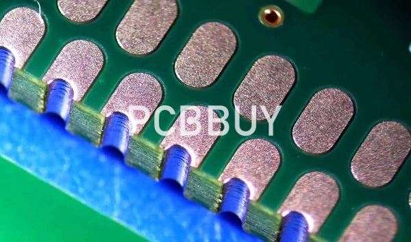
Plated half holes are available in both standard PCB and advanced PCB. For standard PCB service, the minimum diameter of castellated holes is 0.6 mm. If you need smaller castellated holes please ask our sale to offer advanced PCB service. And the minimum distance between two Plated half holes is 0.55 mm. Through connecting the PCBs together directly, the whole system is considerably thinner than a comparable connection with multi-pin connectors. The plated edges are also useful in producing mini PCB modules.
If you are looking for more information about plated half holes of PCB, please check and read the content for more about professional knowledge.
What are the technologies of plated half holes of PCB?
In past, if want to solder a daughter board to a mother board, it requires a board-board connector, which takes much space and increases some project cost. But now if your system can be realized with half-holes technique, you can remove the connector, and make the PCB assembly easy and economical. PCB with plated half-holes on the boundaries stands for the daughter board or surface mount part, will mount flush on the surface of mother board.
Board-to-board PCBs need plated half-holes, which serve as solder mounting device (SMD) terminal pads. Through directly soldering and connecting to the mother PCB, the whole system is considerably thinner than a comparable connection with multi-pin connectors. In one hand, plated-half-hole is an economical connection technique, which can convert the circuit board into surface mounted assembly. In another hand, it can provide a better landing for soldering as it is concave and plated.
How to process plated half holes of PCB?
· Drilling – boiling – picture conversion – pattern boiling – striping – etching – floor layer – surface covering – half holes plating.
· Since plated half-holes PCB is used to mount one PCB immediately on top of another PCB, two conditions are:
· It requires electric contacts, not just external connections;
· The range between the two boards is gap or none.
The half-holes plated are cost-effective linking strategies that transform the circuit board into sub-assembly on the wall. They are typically mainly in fine-pitch SMD or on portable radios or RF assemblies. The panels will provide a perfect soldering landing since they are concave and plated. They are at the borders of the PCB stands for the motherboard or mounting surface pieces flush into the motherboard surface. The only suit would there be no space for air or dust to collect.

What is active half hole of PCB?
If you recall your electronics lessons now, you would also remember the embedded DIP or acrylic DIP circuits that you had (PDIP). These modules are usually considered to be installed on proof-of-concept breadboards but are generally found in actual PCBs. The DIP kit is standard for organic compounds, such as op-amp bundles, low voltage controls, and many other similar components. Other parts such as transistors, higher voltage regulators, quartz resonators, higher power LEDs, and several others may be supplied in a zigzag inline (ZIP) or transistor contour (TO) kit. Like axial or radial passive half-hole technology, these other packages are often mounted onto a PCB.
Plated half-holes came when manufacturers were more worried about the mechanical stability of electrical devices and less concerned about esthetics and signal accuracy. The emphasis was less on space reduction in the modules and no issue with signal integrity. Later on, as the central stage started to be played by power usage, signal integrity, and board room, designers wanted components of the same electrical versatility in a smaller box. This is where elements of the surface mount fall in.
What are the specifications of half hole of PCB?
1. Half hole printed circuit board
2. Cost-effective, high quality
3. PCB OEM & ODM are available
4. ISO9001, UL, RoHS certificated
Plated half holes boards are applied to industries such as: telecommunication, computer application, industrial control, power, automobile and high-end consumer electronics, and so on.
What are the applications of half hole of PCB?
More and more often plated slots, plated edges or even completely plated outlines are required for PCB boards. While plated slots are relatively easy to produce. Plated Half-holes PCBs are predominantly used for board-to-board connections, mostly where two printed circuit boards with different technologies are combined. The half-holes PCBs can be standard PCBs and advanced PCBs. They may be included as a part of the board circuitry such accessing parts on a daughter board. The board-to-board PCBs need plated half-holes, which serve as SMD connection pads. Through directly connecting the PCBs together, the whole system is considerably thinner than a comparable connection with multi-pin connectors. The solder paste will climb onto the half holes when the half hole circuit board go through reflow soldering machine. The cooled solder paste on the half hole walls looks shining.
Applications of Half Holes PCBs
Plated half holes are economical connection techniques, which transform the board into a surface mount sub-assembly. They are frequently used as breakout circuits for find-pitch SMD components or on small radio or RF assemblies. Since they are plated and concave, these PCBs provide better landings for soldering. Their position on the boundaries of the board signifies that the surface mount components or daughter board will mount flush on the motherboard surface. There will be no space for dust or moisture to gather once the unit is place. Castellated holes PCBs (Half-holes PCBs) are widely applied for microcontroller modules, display, HF or ceramic modules which are soldered to the base PCBs.
Industry Category


