How to Improve PCB Design with 3 Types of PCB Shielding?
By:PCBBUY 09/28/2021 09:12

PCB can be victimized by incoming electromagnetic interference (EMI) and also affect other electronics with outgoing EMI. There are many solutions to block the interference, including the use of metal shields or cans. The key is to use these different types of shielding in analog layouts, starting first with good PCB design techniques. .
In this passage, we will focus on the types of PCB shielding. If you are going to learn how to improve PCB design, please check and read the content below for more information.

What are the 3 main types of PCB Shielding?
1. RF Shielding
Electromagnetic Interference shielding or EMI shielding that impedes radio frequencies and electromagnetic radiation is called RF shielding. This type of shielding reduces the coupling of radio waves, electromagnetic fields and electrostatic. A conductive enclosure used to block electrostatic fields is also known as a Faraday cage.
2. Arduino Shielding
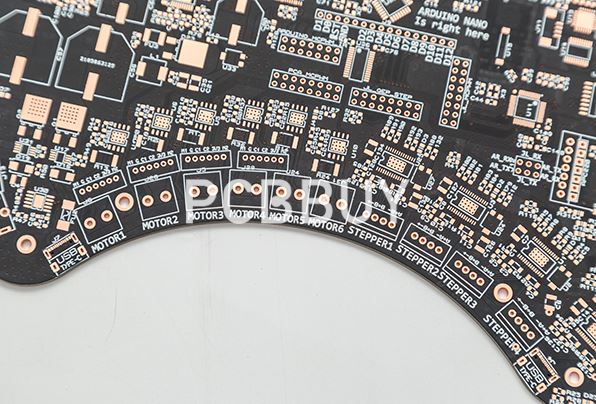
The Arduino EMI PCB shield is a board that can be mounted on top of the Arduino board. Its shield pins are inserted into the sockets located down both sides of the Arduino board. Arduino has a large, range of shields designed for prototyping.
3. EMC Shielding
EMC Shielding is any method used to protect a sensitive signal from external electromagnetic signals, or preventing a stronger signal from leaking out and interfering with surrounding electronics. It can cover PCB elements such as IC chips and active components, or connectors and cables between PCBs.
EMC is short for Electro Magnetic Compatibility, which means that a circuit has been designed with this prevention of disruption by shielding. Electromagnetic frequencies can affect many sensitive electronics, and can cause a wide variety of different issues from a simple hiss on a communication line, to a total disruption of a safety-critical signal.

How to process the PCB Shielding in PCB design?
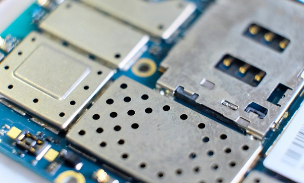
Metal shields or cans are added to shield a circuit board from EMI, in order to contain critical areas on the PCB. Shielding covering four sides and the top is soldered down to the ground plane under the components. This type of shielding is called a Faraday cage. Ideally the shield should completely enclose components to block off all emissions. However, shield openings are required for thermal cooling, seams, adjustments, and solder points to the board.
Board Layer Stackup
How the layers are configured in your PCB stackup is an essential first step in the control of EMI. While it may seem attractive to reduce the layer count to reduce manufacturing expenses, that strategy may damage the signal integrity of the board. High-speed signals, sensitive analog nets, and noisy power circuitry all need to be isolated from each other, and that may require additional layers in the stackup. It is also important to provide enough layers for ground planes to shield these signal layers from emitting or being victimized by EMI.
Component Placement
How components are placed will also make a big difference in how the board is shielded against EMI problems. Here are some general guidelines to keep in mind:
To ensure that your design is EMC compliant, it is important to keep PCB components grouped according to their function. You don’t want digital circuitry to flow through an analog portion of the board, except for those signals that directly connect the two together.
Power and Ground Planes
Metal planes in the board layer stackup provide a lot of shielding, and it is a good practice to route sensitive signals on a layer between two ground plane layers in a stripline configuration. In addition, here are some other guidelines to remember when designing your planes:
Use separate planes for analog and digital grounds to keep their noises separate. Provide clear digital signal return paths in the planes that do not flow through areas of analog circuitry. Be careful with split planes, cutouts, or holes in the planes that allow EMI through and can create obstacles for clear signal return paths.
Avoid using split planes, but if they are necessary, ensure that the splits only connect to each other at one point. Multiple connection points between split planes can create loops resulting in an antenna that radiates EMI.

What are the guidelines of PCB Shielding to improve PCB design?
How to design a board with low or absolutely zero electromagnetic interference? Well, it isn’t impossible. The below design practices will make sure you do not create antennas, which will emit electromagnetic energy. These best design practices will reduce the length and area of the potential signal return paths that may increase unwanted EM emissions. The multi-layers stack-up
Trace spacing and layout
Traces are the conductive paths that carry current from the driver to the receiver on the PCB. When these traces come across any bend or cross, they form a fully radiating antenna. Some common trace design rules are:
Ground planes
A ground with low inductance value is a crucial element during PCB designing for mitigating EMC problems. Increasing the ground area on a PCB reduces the ground inductance in the system, hence EM emission and crosstalk too. Several approaches are available when we need to connect the signals to the ground, but what is best? Before jumping to the best PCB design approach, let us discuss what is not at all acceptable? Never connect the PCB components randomly to the ground points. So, what is the recommended design approach?
Industry Category


