How to Improve PCB Quality with FPGA PCB Design Guidelines?
By:PCBBUY 12/03/2021 09:13

Just as an example, the development of the FPGA’s constraints may have to begin before the component is connected in the schematic. This may be because the pin function is limited to certain pins. Maybe the FPGA IO has to be configured in a certain way for the part to work which is required by the firmware. Either way, this is a problem which requires swapping back and forth between developing the schematic of a board/product and developing the firmware for it.
Are you going to learn more knowledge of FPGA PCB design? If you are curious about the FPGA PCB design and need the guideline, please check and read the content below in this passage.
What are the considerations of FPGA PCB design?
I’ll assume you have a rough idea of what external parts you need, as they will be highly dependant on what you are trying to accomplish with your design. In addition to design-specific information, there are a few standards external requirements such as programming interface, communications, and power. This article will briefly cover some of these external requirements, but the concentration of this article is how to physically lay-out the FPGA board at a reasonable cost.
Assuming this design will be either a prototype run or possibly a small production run, it makes sense to design your PCB with specific requirements in mind to keep costs reasonable. The two PCB specifications you are most commonly told are the minimum “trace/space” (that is, minimum width of a trace, and minimum spacing between copper features), and the minimum drill size.
As I mentioned in my previous article, I’m often using an overseas PCB fab at 3pcb.com, although many other options are worth trying. They offer a variety of trace/space and drill size options, so I’ll target a 5 mil space/trace with 0.2 mm drill.
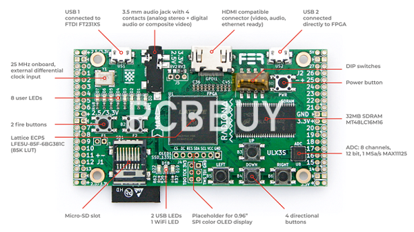
How to design FPGA PCB?
When the goal is first-time success, high quality, and minimal debug effort, design teams must consider a laundry list of items—a list that is especially long for FPGA-based systems. Today, this means a great deal of busy work and attention to minute details. The problems inherent in FPGA-based system designs can be classified into the following categories:
1. Functional – issues that cause the design to not work functionally. For example, if a clock to the FPGA is not coming in through a clock pin specified by the FPGA vendor, the clock cannot be distributed with a reasonable skew, and hence the design will fail to function.
2. Electrical – electrical issues that again cause the board to not work. If a 3.3 V LVTTL signal is connected to an FPGA bank that has a 1.8 V voltage rail, the signal will not function electrically, and so the design will fail.
3. Marginal – issues that allow the board to work most of the time (but cannot be guaranteed to work all of the time). For example, if a clock is connected to a non-clock pin in the FPGA, it cannot be correctly distributed within the FPGA. When this happens, the design may not work at some frequencies, though it may work at certain other frequencies.
Some of the electrical and functional issues require a re-spin of the board. Some of these may be rectified with ‘green wires’ (or wires of your favorite color), but may make the board less robust. Such fixes typically require a re-spin before the board is production worthy. Marginal issues are not only harder to find, but are harder to debug and fix as well. More importantly, the marginal issues are the ones that could show up at a customer site—which makes it critical to put more emphasis on avoiding these

What are the applications of FPGA PCB?
The Altera series FPGA boards are a multiuser, multi-threaded design suited for many markets such as enterprise automation, digital signal processing, and cyber security. These series include FPGA devices with a comprehensive range of I/O expansion for processor-intensive applications. They include:
Intel Stratix 10 FPGA board:
If you need a compact, powerful FPGA for various engineering applications in various industry sectors, this is your board. FPGA boards are helpful in many different applications, including embedded system design and video processing.
Intel Stratix Ge FPGA board:
This board is specifically designed for the aerospace industry, whereas the Stratix 10 FPGA board is a more general-purpose FPGA. The Ge FPGA board has a bit more computational performance and throughput than the Stratix 10 FPGA board. This board can handle a wide range of applications. The board is also suitable for professional design projects.
Stratix 10 GX FPGA board:
The Ge FPGA board is entirely compatible with the Stratix 10 FPGA board, with extra features and more powerful computing performance. These boards are essential in commercial design projects, especially those involving industrial design or consumer products.
Stratix V FPGA boards:
This is a range of FPGA boards based on the Stratix series. The board offers high-performance and advanced features, such as high-speed transceivers and increased connectivity options. It also has a lower power consumption than previous
FPGA boards that were available from Altera. This can be beneficial in specific applications, such as battery-powered devices. However, its design is also essential for industrial design and engineering applications.
Stratix 7 FPGA board:
This is the latest generation FPGA board based on the Stratix series. The Stratix 7 FPGA board is compatible with the previous models (6, 6 E, 6 GX) and has exclusive features. Like its predecessors, it offers high performance and fast computing capabilities. Like other Altera boards, it comes with excellent software support. As a result, we can use the board in both industrial and embedded design projects.
Industry Category


