How to Improve the Design Process with Top 5 PCB Stackup Rules?
By:PCBBUY 10/08/2021 10:19

A stackup is the arrangement of layers of copper and insulators that make up a PCB before designing the final layout of the board. Managing a good stackup is not exactly easy and companies that make multilayer printed circuits such as Proto-Electronics, a European platform dedicated to the rapid prototyping of SMT printed circuits and cross-section components, for professionals, must be at the forefront.
In this passage, we will provide you the methods of PCB stackup rules to improve the design. Check and read our content to learn more about the information of PCB stackup rules.
What are the 5 tips for PCB stackup rules?
1. Determining the layer arrangement
After determining the number the layers, you need to determine how they should be arranged or stacked. Good rules to follow here are:
· Route high-speed on minimum thickness microstrips.
· Place signal layers next to internal power layers for tight coupling.
· Power and ground layers should have minimal spacing between them.
· Avoid having two signal layers adjacent to each other.
· Make the stackup symmetric from the top and bottom layers inward
2. Determining routing and vias
Completing the PCB stackup design is the determination and routing of the traces. This includes determining copper weights, where to put vias and what type of vias to implement. As for all specifications for your design, you should work with your CM in making these determinations as some CMs avoid certain via types, such as via-in-pads.
3. Know the advantages of multilayer PCB stackup
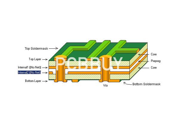
Having multiple layers (see figure 1) increases the board's ability to distribute energy, reduces cross-interference, eliminates electromagnetic interference and supports high-speed signals. While a stackup level allows you to get multiple electronic circuits on a single board through the various layers of PCB board, the structure of the PCB stackup design provides many other advantages:
· A stack of PCB layers can help minimize the circuit vulnerability to external noise, as well as minimize radiation and decrease impedance and crosstalk problems on high-speed systems;
· Good PCB stacking can also contribute to efficient and low-cost final production;
· A correct stack of PCB layers can improve the electromagnetic compatibility of the project.
4. Rules to process best stackup of PCB
The rules and criteria for managing a good stackup are hundreds. Let's just see a few:
· Ground plane boards are better because they allow signal routing in a microstrip or stripline configuration. It also significantly reduces the ground impedance and, therefore, the ground noise;
· High speed signals should be "routed" on intermediate layers located between the various levels. In this way, ground planes can act as a shield and contain the radiation coming from the tracks at high speed
· The signal layers should be very close to each other, even in adjacent planes.
· A signal layer must always be adjacent to a plane
· Multiple ground planes are very advantageous, since they lower the board's ground impedance and reduce radiation in a common way
· The power and mass planes must be rigorously coupled together

5. Routing layer during PCB stackup design process
An electrician installing electrical wiring in a house must follow rules to ensure that the wire will not have sharp bends or become vulnerable to the nails or screws used to install drywall. Running the electrical wire through stud walls requires a consistent approach to the depth and height of the wiring path.
Finding Space for the Ground Plane and Power Plane
Every house has a main electrical service panel or load center that receives incoming electricity from an electrical utility and distributes power to circuits that supply lights, outlets, appliances, and devices. The ground planes and power planes of a PCB provide the same functionality by connecting the circuit to ground and by distributing different onboard voltages to components. As with a service panel, the power and ground planes can contain multiple copper sections that allow circuits and sub-circuits to connect to different potentials.
Protect the Board, Protect the Traces
Professional house painters carefully document the colors and finishes used for ceilings, walls, and trim. On a PCB, the silkscreen layers use text to designate the locations of components on the top and bottom layers. Having the information available through a silkscreen saves a design team from referring back to assembly documents.
Positives for PCB Layer Stackup Organization
As PCB technologies have improved and consumer demands for faster, more powerful products have increased, PCBs have changed from the basic two-layer boards to boards that have four, six, and as many as twelve-to-sixteen layers of dielectrics and conductors. Why increase the number of layers? Having more layers increases the capability of the board to distribute power, reduce cross-talk, eliminate electromagnetic interference, and support high-speed signals. The number of layers used for a PCB depends on the application, the operating frequencies, pin density, and the requirement for signal layers.
Industry Category


