How to Improve the PCB Design through NFC PCB Antenna Design?
By:PCBBUY 12/09/2021 09:25

NFC, while similar in many respects to RFID and has its history based on RFID, it is a separate concept. RFID has passive and active tags, with active tags being read from relatively long distances, NFC, as its name implies, works in the near field region of the electromagnetic field.
Are you going to learn more about NFC PCB antenna design? If you are searching for the professional knowledge of NFC PCB antenna design, please check and read the content below in this passage.
What is the quality of NFC PCB?
The selection of the correct NFC PCB manufacturer is a significant concern. The term quality may signify a range of various things and is not specified and may be vague in itself.
However, in essence, the NFC PCB quality implies that the panel comes in and draws – no mistakes.
· The quality of PCBs might indicate a multitude of aspects:
· Board in the proper size
· All hole drilled and placed precisely
· Test bare board passes
· Minimum bending of the board (although some of this can be due to board design)
· A lot of additional problems.
The performance should always remain excellent and not decline once the primary orders have been acquired successfully.
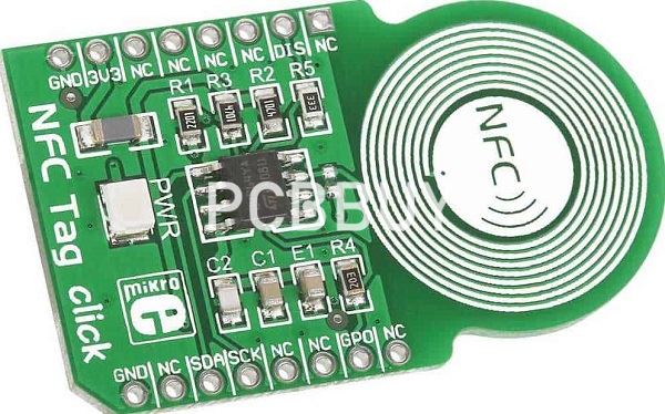
What is the working principle of NFC PCB?
The initiator (emitter) actively produces an RF field via magnetic fields between parallel circuit NFC antennas that may provide a passive goal (Tag).
Emitter antennas and the tag are connected via electrostatic energy, and best this system can be seen as an air-core converter, where the reader acts as a primary winding and the tag as a secondary winding: the alternative charging current through the superior (Emitter) induces an airfield that induces currents into the secondary belt (Tag). The tag may utilize the field current to power itself. In this instance, no battery is needed in reading or write mode to access it. The NFC tag chip gets all power required to function from the viewer’s produced magnetic field via its receiver coil.
What is inductance NFC PCB Antenna?
An NFC tag must have a PCB NFC antenna to connect and be powered. The antenna design process begins with the NFC chip approximate solution and its loop antenna:
· VOC is the open-circuit voltage of the loop antenna caused by a magnetic field
· Ra is the corresponding loop antenna resistance
· La is the comparable loop antenna inductance
· Rs is the NFC chip’s serial equivalent resistance
· Cs is the conventional equivalent NFC chip tuning capability
An inductance La with a very modest loss resistors Ra may define the antenna. When the transmitter in the loop antenna induces a magnetic field, there is a current there, and an open-circuit voltage Voc emerges at its terminals. The resistive input Rs and a built-in tuning condenser Cs may define the NFC PCB chip.

What are the applications of NFC PCB?
NFC is an emerging technology that needs to link electrical devices wirelessly. To communicate with hardware devices suitable with NFC and enable new services, such as contactless payment, NFC has been increasingly implemented into devices.
Because NFC tags do not require a power source to be included since they may be driven by the energy the reader emits, it may take extremely basic operating systems such as electric powered tags, NFC stickers, NFC card manufacturers, and even rings.
How to process open source of NFC PCB?
Certain manufacturers offer entire solutions for electrical developers, such as designs, application instructions, and even EDA files, to assist the installation of their NFC ICs.
This is the case with NXP, which sells integrated circuits for their NFC range NTAG is a comprehensive handbook with NFC antenna design guidelines and excellent computation software for rectangular and circular antennas, Gerber and Eagle files for various antenna classes.
NXP gives the Eagle data of an antenna produced by its engineers and already implemented in some of its devices for this class. The key benefit of this design is the simulation, correction, and optimization.
Industry Category


