How to Install Solidworks PCB & What Are the Basics of It?
By:PCBBUY 12/31/2021 09:47

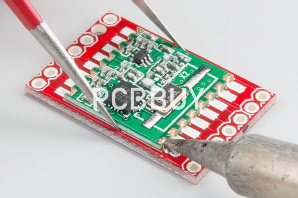
SOLIDWORKS PCB is a professional standalone PCB design tool capable of meeting the demands of today’s products, which allows you to develop the most efficient schematics for your board layouts. Integration of PCB design seamlessly is with SOLIDWORKS CAD, with a managed ECO change process and distinct workflows to keep you at your most productive.
In this passage, we are providing all the details of Solidworks PCB. If you are searching for more information about Solidworks PCB, please check and read the content below for professional knowledge.
What are the basics and history of Solidworks PCB?
It's a well-accepted fact that electrical design (ECAD) and mechanical design (MCAD) disciplines are fundamentally (and significantly) different from each other. Their design tool suites echo this difference.
To bridge that gap, SOLIDWORKS PCB was created with its roots in Altium Designer. Dassault developed in cooperation with Altium Inc. to smoothly bring together the ECAD and MCAD worlds.
For many years, previous attempts to bridge these worlds were focused on the simple translation of the primitives from one tool suite to another. Though universal 2D formats, like DWG, DXF, and IDF, existed, they could not capture all the necessary details. In most cases, manual duplication for each tool was required, making it extremely difficult to keep mechanical representations in sync across various tools.
In 2008, Altium Inc. revolutionized the ECAD industry by introducing an easy to use 3D modeling in their layout tool, which took advantage of a universal 3D mechanical format called STEP. Altium Designer was then able to pass graphical information to and from the MCAD tool readily.
As this capability developed, it allowed the ECAD and MCAD worlds to pass information back and forth in real-time.

What are the challenges of Solidworks PCB?
Despite efforts over the years, collaboration between MCAD and ECAD workflows has been difficult. Mechanical and electrical engineers still have to exchange design information in various incompatible file formats via email or other data-sharing methods. This makes for a laborious process in which much is lost in translation.
For example, a mechanical engineer creates a 2D footprint of the board outline containing locations of mounting holes, connectors and keep-out areas. This information is then sent to the electrical engineer in the form of a PDF or DXF. The electrical engineer imports or recreates the outline inside the PCB design software to being the route and layout process in conjunction with the schematic. The completed design is then sent back to the mechanical engineer in various file formats (STEP, IDF, DXF, etc.) to ensure the board fits in the enclosure.
There is little intelligence in these file formats and, inevitably, changes have to be made. Even a simple revision, such as adjusting the location of a component or even modifying the text on the silkscreen, could cost $1,500 or more. Before all is said and done, a typical circuit board design may undergo numerous costly and time-consuming revisions.

What are the features of Solidworks PCB?
SOLIDWORKS PCB integrates a lot of PCB design tools, which features an easy-to-use and modern design interface. It has a user interface feature, which supports a workflow that is smooth and intuitive. This can be seen in the PCB design solidworks, schematic, and even in the design release stage. These features include:
· A refined menu system of ribbon-style
· Multi-tab, flexible, design editor windows
· User configuration preferences
· Dockable panels, which helps when working with design documents
· A complete set of command shortcut keys
· web-based and context-sensitive help reference
While moving between tasks in the design workflow of SOLIDWORKS PCB, its system responds to the present requirements. It does this by opening the ribbon menu set, panels, and design editors, which you may need for the current task. The design environment maintains a consistent feel and look, and changes dynamically to present the right windows and tools as you design. The elements of the user interface are nevertheless consistent when it comes to function, positioning, and style.
· You can open multiple documents for editing, with each giving you a separate Document Tab, which can be found on top of the workspace.
· While switching between different documents, for example from a PCB design to a schematic sheet, the tool options, and ribbon menu will change automatically.
· The commands seen in the File tab of the ribbon remain unchanged, regardless of the type of document.
· Workspace controls like panels can be docked along any of the workspace’s edges, at the side, or float on top of the application.
Industry Category


